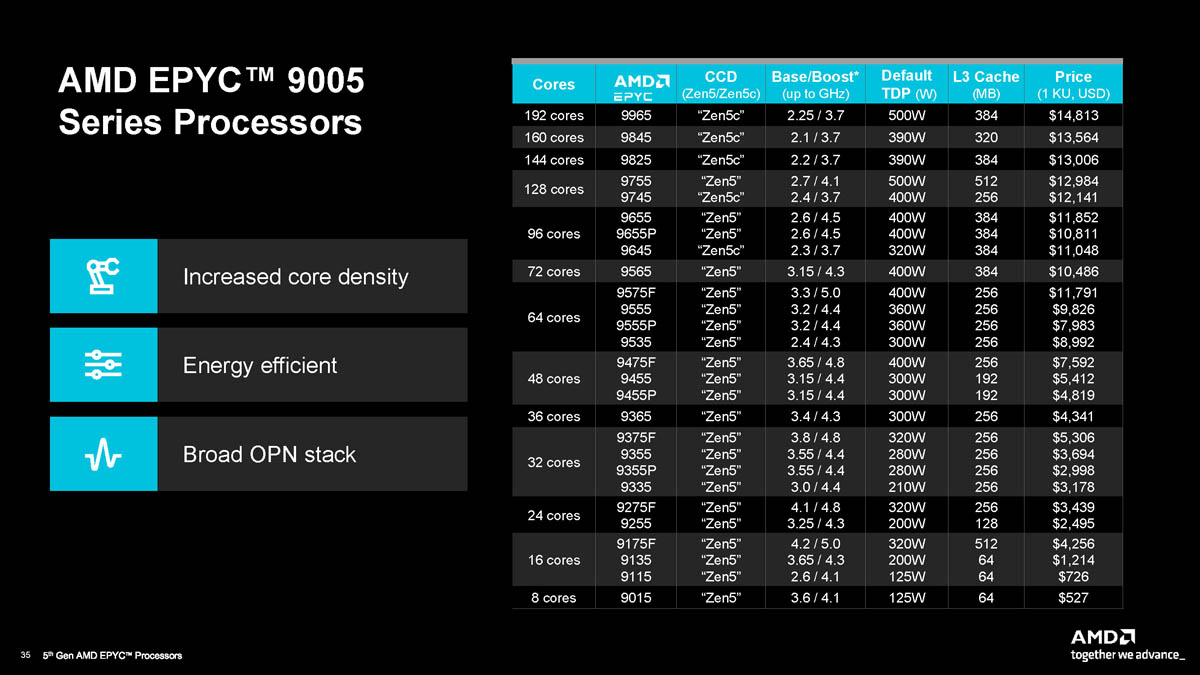
The weirdest one of the bunch is the AMD EPYC 9175F: 16 cores with 512MB of L3 cache! Presumably this is for customers trying to minimize software costs that are based on "per-core" licensing. It really doesn't make much sense to have so few cores at such an expense, otherwise. Does Oracle still use this style of licensing? If so, they need to knock it off.
The only other thing I can think of is some purpose like HFT may need to fit a whole algorithm in L3 for absolute minimum latency, and maybe they want only the best core in each chiplet? It's probably about software licenses, though.
Another good example is any kind of discrete event simulation. Things like spiking neural networks are inherently single threaded if you are simulating them accurately (I.e., serialized through the pending spike queue). Being able to keep all the state in local cache and picking the fastest core to do the job is the best possible arrangement. The ability to run 16 in parallel simply reduces the search space by the same factor. Worrying about inter CCD latency isn't a thing for these kinds of problems. The amount of bandwidth between cores is minimal, even if we were doing something like a genetic algorithm with periodic crossover between physical cores.
Plenty of applications are single threaded and it's cheaper to spend thousands on a super fast CPU to run it as fast as possible than spend tens of thousands on a programmer to rewrite the code to be more parallel.
And like you say, plenty of times it is infeasible to rewrite the code because its third party code for which you don't have the source or the rights.
A couple years ago I noticed that some Xeons I was using had a much cache as the ram in the systems I had growing up (millennial, so, we’re not talking about ancient commodores or whatever; real usable computers that could play Quake and everything).
But 512MB? That’s roomy. Could Puppy Linux just be held entirely in L3 cache?
CCDs can't access each other's L3 cache as their own (fabric penalty is too high to do that directly). Assuming it's anything like the 9174F that means it's really 8 groups of 2 cores that each have 64 MB of L3 cache. Still enormous, and you can still access data over the infinity fabric with penalties, but not quite a block of 512 MB of cache on a single 16 core block that it might sound like at first.
Zen 4 also had 96 MB per CCD variants like the 9184X, so 768 MB per, and they are dual socket so you can end up with a 1.5 GB of total L3 cache single machine! The downside being now beyond CCD<->CCD latencies you have socket<->socket latencies.
Hmm. Ok, instead of treating the cache as ram, we will have to treat each CCD as a node, and treat the chip as a cluster. It will be hard, but you can fit quite a bit in 64MB.
Firmware is using cache as RAM (e.g. https://www.coreboot.org/images/6/6c/LBCar.pdf) to do early init, like DRAM training. I guess later things in the boot chain rely on DRAM being set up probably though.
I would be pretty curious about such a system. Or, maybe more practically, it might be interesting to have a system pretends the L3 cache is ram, and the ram is the hard drive (in particular, ram could disguise itself as the swap partition, to so the OS would treat is as basically a chunk of ram that it would rather not use).
> The RAMpage memory hierarchy is an alternative to a conventional cache-based hierarchy, in which the lowest-level cache is managed as a paged memory, and DRAM becomes a paging device.
So, essentially, you're just doing cache eviction in software. That's obviously a lot of overhead, but at least it gives you eviction control. However, there is very little to do when it comes to cache eviction. The algorithms are all well known and there is little innovation in that space. So baking that into the hardware is always better, for now.
Many algorithms are limited by memory bandwidth. On my 16-core workstation I’ve run several workloads that have peak performance with less than 16 threads.
It’s common practice to test algorithms with different numbers of threads and then use the optimal number of threads. For memory-intensive algorithms the peak performance frequently comes in at a relatively small number of cores.
Is this because of NUMA or is it L2 cache or something entirely different?
I worked on high perf around 10 years ago and at that point I would pin the OS and interrupt handling to a specific core so I’d always lose one core. Testing led me to disable hyperthreading in our particular use case, so that was “cores” (really threads) halfed.
A colleague had a nifty trick built on top of solarflare zero copy but at that time it required fairly intrusive kernel changes, which never totally sat well with me, but again I’d lose a 2nd core to some bookkeeping code that orchestrated that.
I’d then tasksel the app to the other cores.
NUMA was a thing by then so it really wasn’t straightforward to eek maximum performance. It became somewhat of a competition to see who could get highest throughout but usually those configurations were unusable due to unacceptable p99 latencies.
Windows server and MSSQL is per core now. A lot of enterprise software is. They are switching to core because before they had it based on CPU sockets. Not just Oracle.
Phoronix recently reviewed the 196 core Turin Dense against the AmpereOne 192 core.
* Ampere MSRP $5.5K vs $15K for the EPYC.
* Turin 196 had 1.6x better performance
* Ampere had 1.2x better energy consumption
In terms of actual $/perf, Ampere 192 core is 1.7x better than Turin Dense 196 core based on Phoronix's review.
So for $5.5k, you can either buy an AmpereOne 192 core CPU (274w) or a Turin Dense 48 core CPU (300w).
Ampere has a 256 core, 3nm, 12 memory channel shipping next year that is likely to better challenge Turin Dense and Sierra Forest in terms of raw performance. For now, their value proposition is $/perf.
Anyway, I'm very interested in how Qualcomm's Nuvia-based server chips will perform. Also, if ARM's client core improvements are any indication, I will be very interested in how in-house chips like AWS Graviton, Google Axion, Microsoft Cobalt, Nvidia Grace, Alibaba Yitian will compete with better Neoverse cores. Nuvia vs ARM vs AmpereOne.
This is probably the golden age of server CPUs. 7 years ago, it was only Intel's Xeon. Now you have numerous options.
AMD also wins on perf/Watt which is pretty notable for anyone who still believed that X86 could never challenge ARM/Risc in efficiency. These days, lot of data centers are also more limited by available Watts (and associated cooling) which bodes well for Turin.
> In terms of actual $/perf, Ampere 192 core is 1.7x better than Turin Dense 196 core based on Phoronix's review.
You're comparing it to the highest MSRP Turin, which doesn't have the highest performance/$. People buy that one if they want to maximize density or performance/watt, where it bests Ampere. If you only care about performance/$ you would look at the lower core count Zen5 (rather than Zen5c) models which have twice the performance/$ of the 192-core 9965.
Doing the same for Ampere doesn't work because their 192-core 3.2GHz model is very nearly already their peak performance/$.
700+ threads over 2 cores, can saturate 2 400gbe Nic's 500 wats per chip (less than 2 wats per thread)... All of that in a 2U package.... 20 years ago that would have been racks of gear.
I think those really 2 watts per thread are a lot more important than what us home users usually think. Having to deliver less power and having to dissipate less watts in form of heat in a data centre are really good news to its operative costs, which is usually a lot bigger than the cost of the purchase of the servers
On the other hand, at the time we would have expected twenty years of progress to make the cores a thousand times faster. Instead that number is more like 5x.
On a different hand the way things were scaling 20 years ago (1ghz took 35 watts) we'd have 5,000W processors - instead we have 196 for 300 watts. If these are anything like ThreadRipper I wonder if they can unlock to 1000W with liquid cooling. On the flip side we are rolling about 1 to 2 watts per core which is wild. Also, can't some of these do 512bit math instructions instead of just 32bit?
Well, a 286 was about 3 watts right? So if our medium point is 35 watts then the final would be 400 watts.
Or if our medium point is a 60 watt pentium 4 then our final point would be a 1200 watt single core with multiple millions of times the performance, and dropping down to 300 watts would still be crazy fast.
I often think about huge, fancy cloud setups literally costing silly money to run, being replaced by a single beast of a machine powered by a modern, high core count CPU (say 48+), lots of RAM and lots of high performance enterprise-grade SSD storage.
(Oftentimes part of the reason the huge, fancy cloud setup costs more is that any component can fail, all the way down to the region-level, without loss of service.)
The difference in throughput for local versus distributed orchestration would mainly come from serdes, networking, switching. Serdes can be substantial. Networking and switching has been aggressively offloaded from CPU through better hardware support.
Individual tasks would definitely have better latency, but I'd suspect the impact on throughput/CPU usage might be muted. Of course at the extremes (very small jobs, very large/complex objects being passed) you'd see big gains.
By way of a single example, we've been migrating recently from spark to duckdb. Our jobs are not huge, but too big for a single 'normal' machine. We've gone from a 2.5 hour runtime on a cluster of 10 machines (40,vCPU total) to a 15 minute runtime on a 32vCPU single machine. I don't know for sure, but I think this is largely because it eliminates expensive shuffles and serde. Obviously results vary hugely depending on workload, and some jobs are simply too big even for a 192 core machine. But I suspect a high proportion of workloads would be better run on single large machines nowadays
A cluster of 10 machines with 40 vCPUs in total would equate to 4 vCPUs per machine. I am not familiar with Spark internals but in the realm of distributed databases such a setup would generally make no sense at all (to me). So I think you're correct that most of the overhead was caused by machine-to-machine byte juggling. 4 vCPUs is nothing.
I suspect you would be able to cut down the 2.5hr runtime dramatically even with the Spark if you just deployed it as a single instance on that very same 32vCPU machine.
Your measuring wall time, not CPU time. It may be that they are similar, but I'd suspect you aren't loading the worker nodes well. If the savings are from the reduced shuffles & serde, it's probably something you can measure. I'd be curious to see the findings.
I'm not against using simple methods where appropriate. 95% of the companies out there probably do not need frameworks like spark. I think the main argument against them is operational complexity though, not the compute overhead.
When you talk between remote machines, you have to translate to a format that can transmitted and distributed between machines(serialization). You then have to undo at the other end(deserialization). If what you are sending along is just a few floats, that can be very cheap. If you're sending along a large nested dictionary or even a full program, not so much.
Imagine an example where you have two arrays of 1 billion numbers, and you want to add them pairwise. You could use spark to do that by having each "task" be a single addition. But the time it would take to structure and transmit the 1 billion requests will be many multiples of the amount of time it would take to just do the additions.
Nowadays very much most services can fit on single server and serve millions of users a day. I wonder how it will affect overly expensive cloud services where you can rent a beefy dedicated server for under a grand and make tens of thousands in savings (enough to hire full time administrator with plenty of money left for other things).
Indeed: the first dual core server chips only launched in 2005 afaik with 90nm Denmark/Italy/Egypt Opterons and Paxville Xeons but on the Intel side it wasn't until 2007 when they were in full swing.
first dual core server chips show up generally available in 2001 with IBM POWER4, then HP PA-RISC ones in 2004, and then Opterons which was followed by "emergency" design of essentially two "sockets" on one die of of NetBurst dual core systems.
Also, I raised the question at https://retrocomputing.stackexchange.com/q/30743/3722 and one of the answers points out the 1984 Rockwell R65C29 Dual CMOS Microprocessor. It was two standard 6502 on the same die using the same bus to access the same memory... and of course IBM mainframes did it decades before.
Depends on your definition. The 8271 wasn't programmable by anyone but Intel (at least, they never made that a market option), and the second core was more of a bit-oriented coprocessor, sorta like saying the 80486 is a 2-core processor because of the FPU.
Ehhhh the MAJC 5200 was generally available in 1999 and I am sure even older designs could be found if we were to dig deep enough. Their market share would also need some digging too.
To quote the announcement: "two VLIW (very long instruction word) microprocessors on a single piece of silicon"
By the time of XVR GPUs Sun was pretty much exiting the workstation market, and unlike Elite3D and Creator3D the competition has widened for "good enough" PC alternatives using Nvidia and similar chips
1-3rd gen Epycs can be had super cheap, but the motherboards are expensive.
Also not worth getting anything less than 3rd gen unless you're primarily buying them for the pcie lanes and ram capacity - a regular current gen consumer CPU with half - a quarter of the core count will outperform them in compute while consuming significantly less power.
Yes. It keeps the board from booting if the firmware is replaced with a version not signed by the board manufacturer (i.e. so an attacker can’t replace it with a version that does nefarious things). Preventing CPU reuse in other boards is just an (unintentional?) side effect.
The reason for this is that CPU upgrades on the same board were/are very viable on SP3.
Doing that on Intel platforms just wasn't done for basically ever, it was never worth it. But upgrade to Milan from Naples or Rome is very appealing.
So SP3 CPUs are much more common used than the boards, simply because more of them were made. This is probably very bad for hobbyists, the boards are not going to get cheap until the entire platform is obsolete.
Lots of great second hand hardware to be had on ebay. Even last gen used CPUs, as well as RAM, at much less than retail.
However when you end up building a server quite often the motherboard + case is the cheap stuff, the CPUs are second in cost and the biggest expense can be the RAM.
IMO, 1st gen Epyc is not any good, given that 2nd gen exists, is more popular and is cheap enough (I actually have epyc 7302 and MZ31-AR0 motherboard as homelab). Too low performance per core and NUMA things, plus worse node (2nd gen compute is 7nm TSMC)
ChipsAndCheese is one of the few new tech publications that really knows what they are talking about, especially with these deep dive benchmarks.
With the loss of Anandtech, TechReport, HardCOP and other old technical sites, I'm glad to see a new publisher who can keep up with the older style stuff.
Chips and Cheese most reminds me of the long gone LostCircuts. Most tech sites focus on the slate of application benchmarks, but C&C writes, and LC wrote, long form articles about architecture, combined with subsystem micro-benchmarks.
Oracle can charge $40-$100k+ for EE including options per core (times .5)...and some workloads are very cache sensitive. So a high cache, high bandwidth, high frequency, high memory capacity 16 core CPU[1] (x2 socket) might be the best bang for their buck for that million dollar+ license.
Surely that's a good reason for Oracle to increase their prices even more, leading to a cat-and-mouse game between CPU makers and software license sellers.
Oh yes, this cat-and-mouse game has been going on for more than a decade. But despite that, for any given time and license terms, there is a type of CPU that is optimal for performance/licensing costs, and when the license is as expensive and widely used as it is, it makes sense to sell CPUs for that specific purpose.
The topology of that part is wild, it's physically the same silicon as the 128-core part but they've disabled all but one core on each compute chiplet. 112 cores are switched off to leave just 16 cores with as much cache as possible.
Inter-core latency will be rough since you'll always be hitting the relatively slow inter-chiplet bus, though.
Does anyone know if modern AMD chips allow mapping the L3 cache and using it as TCM instead of cache? I know older non-X86 processors supported this (and often booted into that mode so that the memory controllers could be brought up), but not sure if it's possible today. If so, that would sure make for some interesting embedded use cases for a large DRAM-less system...
> AMD has ported early AGESA features to the PSP, which now discovers, enables and trains DRAM. Unlike any other x86 device in coreboot, a Picasso system has DRAM online prior to the first instruction fetch.
Perhaps they saw badly trained RAM as a security flaw? Or maybe doing it with the coprocessor helped them distribute the training code more easily (I heard a rumour once that RAM training algos are heavily patented? Might have imagined it).
> The system we had access to was running 6000MT/s for its memory, and DDR5-6000 MT/s is what most systems will support in a 1 DIMM per channel configuration. Should you want to run 2 DIMMs per channel, then your memory speeds drop to 4400 MT/s; and if you run 1 DIMM per channel in a motherboard with 2 DIMMs per channel then expect 5200 MT/s for your memory speed.
150ns is actually surprisingly high! I didn't realize it was so bad. That's about 2-3x as much latency as fetching from DRAM based on what I see in peoples AIDA64 results.
Not sure if this comment was about to come out as snarky but the parent rightfully pointed out the not so obvious design of EPYC CPUs. CCD is a NUMA in disguise.
Doubtful, the 350W threadripper parts don’t run particularly hot with normal desktop cooling. I’ve overclocked a 7975WX with an unrestricted power limit, and could dissipate over 800W while keeping it below 90C (admittedly, with water cooling). 500W with server cooling (super high RPM forced air) shouldn’t be a problem.
It is high, but it probably can sustain much higher all core frequency compared to 7950x3D (or 7950x). If nothing else, it has a bigger die and heat spreading to pull heat from, it should be easier to maintain thermal headroom on the EYPC chip.
That being said, it looks most probable what a 9175F is just a 9755 (their absolute max full size Zen5 core part) with nearly all (7/8) of their cores per CCD disabled in order to get all 512MB of cache. This means that there's a lot of extra interconnect being kept running per core which certainly would contribute to the higher TDP.
Of course, in principle this should also mean that each core (which should basically have all of a CDD's IO and cache available to it) should be screaming fast in real terms.
Of course finally, TDP is a totally fluffy number. The TDP of the 7950X3D is most probably as low as it is because of how much internal thermal resistance (the extra V-Cache layer) it has. Part of it's lower TDP isn't because "it's efficient", part of it is because "if we run it hotter, we'll melt it". The TDP for the 7950X for example is 170W.
that's the processor you're supposed to buy only if you are paying $10000 per core per year for some ridiculously expensive enterprise software. the extra power comes from all the extra memory channels and cache
The cores are spread out over roughly 1200 mm² of silicon and the IO die seems to have grown again (maybe 500ish mm²?). So at just 0.3 W/mm² this is pretty cozy. The desktop parts have 3x higher power density.
The H100 has 16,000 cuda cores at 1.2ghz. My rough calculation is it can handle 230k concurrent calculations. Whereas a 192 core avx512 chip (assuming it calculates on 16 bit data) can handle 6k concurrent calculations at 4x the frequency. So, about a 10x difference just on compute, not to mention that memory is an even stronger advantage for GPUs.
A Zen 5 core has four parallel AVX-512 execution units, so it should be able to execute 128 16-bit operations in parallel, or over 24k on 192 cores. However I think the 192-core processors use the compact variant core Zen 5c, and I'm not sure if Zen 5c is quite as capable as the full Zen 5 core.
Right, I found this interesting as a thought exercise and took it from another angle.
Since it takes 4 cycles to execute FMA on double-precision 64-bit floats (VFMADD132PD) this translates to 1.25G ops/s (GFLOPS/s) per each core@5GHz. At 192 cores this is 240 GFLOPS/s. For a single FMA unit. At 2x FMA units per core this becomes 480 GFLOPS/s.
For 16-bit operations this becomes 1920 GFLOPS/s or 1.92 TFLOPS/s for FMA workloads.
Similarly, 16-bit FADD workloads are able to sustain more at 2550 GFLOPS/s or 2.55 TFLOPS/s since the FADD is a bit cheaper (3 cycles).
This means that for combined half-precision FADD+FMA workloads zen5 at 192 cores should be able to sustain ~4.5 TFLOPS/s.
Nvidia H100 OTOH per wikipedia entries, if correct, can sustain 50-65 TFLOP/s at single-precision and 750-1000 TFLOPS/s at half-precision. Quite a difference.
The execution units are fully pipelined, so although the latency is four cycles, you can receive one result every cycle from each of the execution units.
For a Zen 5 core, that means 16 double precision FMAs per cycle using AVX 512, so 80gflop per core at 5ghz, or twice that using fp32
You're absolutely right, not sure why I dumbed down my example to a single instruction. Correct way to estimate this number is to feed and keep the whole pipeline busy.
This is actually a bit crazy when you stop and think about it. Nowadays CPUs are packing more and more cores per die at somewhat increasing clock frequencies so they are actually coming quite close to the GPUs.
I mean, top of the line Nvidia H100 can sustain ~30 to ~60 TFLOPS whereas Zen 5 with 192 cores can do only half as much, ~15 to ~30 TFLOPS. This is not even a 10x difference.
I agree! I think people are used to comparing to a single threaded execution of non-vectorized code, which is using .1% of a modern CPU's compute power.
Where the balance slants all the way towards gpus again is the tensor units using reduced precision...
They're memory bandwidth limited, you can basically just estimate the performance from the time it takes to read the entire model from ram for each token.
The criticism is about "EPYC" not about the codenames. That brand name has been used since 2017 but if you don't know that, it sounds quite gamery nowadays.
Admittedly I also have no idea why Intel calls theirs Xeon, which sounds like misspelled xenon. But then it might be a proper Greek word?
AMD CPUs have pretty small numbers for that, e.g. 100-000000651 or 100-000000789. They almost look wrong with so many zeroes. Zen/+/2 parts have part numbers like YD160XBCM6IAE (which is similar to the part numbers of much older AMD CPUs, which is apparently the AMD Ordering Part Number, OPN, scheme, and every digit codes information about the CPU). Zen 3 started with the new scheme, which just seem to be sequential development numbers. E.g. 3800X is 100-000000022. Here's a list: https://mkdev.info/?p=1245
Intel's naming isn't great, but it's pretty clear. Look at Wikipedia's List of Intel Processors[1] and for 14 generations since 2010, the higher the model number, the faster the processor. The model number like 13700 starts with the generation (13th) and then place in that (700 is upper-mid). Then a capital letter indicating something about form factor.
Compare with List of AMD processors[2] and a "70xx" model could be a Zen Naples Epic, A Zen 2 Mendocino Ryzen, a Zen 2 Rome Epyc, a Barceló-R Ryzen Zen 3, a Milan Epyc Zen 3, a Rembrandt-R Zen 3+, a Zen 4 Raphael Ryzen or Storm Peak Threadripper, or a laptop Ryzen. Wikipedia people can't even put these into a table to compare them, it's pages of random names and overlapping/re-used numbers.
Apple, as usual, have M1, M2, M3 and each one has plain/pro/max/ultra.
Civ 6 really doesn't utilize cores as much as one would think. I mean it'll spread the load across a lot of threads, sure, but it never seems to actually... use them much? E.g. I just ran the Gathering Storm expansion AI benchmark (late game map completely full of civs and units - basically worst case for CPU requirements and best case for eating up the multicore performance) on a 7950X 16 core CPU and it rarely peaked over 30% utilization, often averaging ~25%. 30% utilization means a 6 core part (barring frequency/cache differences) should be able to eat that at 80% load.
Whether the bottleneck is memory bandwidth (2x6000 MHz), unoptimized locking, small batch sizes, or something else it doesn't seem to be related to core count. It's also not waiting on the GPU much here, the 4090 is seeing even less utilization than the CPU. Hopefully utilization actually scales better with 7, not just splits up a lot.
> 16 core CPU and it rarely peaked over 30% utilization, often averaging ~25%. 30% utilization means a 6 core part (barring frequency/cache differences) should be able to eat that at 80% load.
As a rule I wouldn't be surprised if 90% of the stuff Civ 6 is doing can't be parallelized at all, but then for that remaining 10% you get a 16x speedup with 16 cores. And they're underutilized on average but there are bursts where you get a measurable speedup from having 16 cores, and that speedup is strictly linear with the number of cores. 6 cores means that remaining 10% will be less than half as fast vs. having 16 cores. And this is consistent with observing 30% CPU usage I think.
If only 10% of the workload can be parallelized, then the best case parallelization speed up is only 10%. That doesn’t line up with the GP’s claim that Civ6 benefits from more cores.
My rule is more like I’d be willing to bet even odds that this could be sped up 100x with the right programmers focused on performance. When you lack expertise and things work “well enough” that’s what you get. Same for games or enterprise software.
That's what we get in a market dominated more by the need to release before the competition rather than taking some time to optimize software. If it's slow, one can still blame the iron and users who don't upgrade it.
That's the usual case when vid3o g4mes are "CPU limited". One has to just look whether the game does anything high-level that other games didn't do 10 years ago. Reasonable hardware limitations related to the CPU have normally to do with complex physics effects or unusually large crowds of NPCs. (Many games are CPU limited even for fairly small crowds because their engine isn't optimized for that purpose.)
Old habit. I'm a kid of the 1990s, and we were convinced there wasn't anything cooler than a) video games and b) replacing letters with numbers. It retrospect, we might have been a little biased.
Well, just for future reference; if you're a kid of the 90s, you're well into your 30s now.
It's weird/juvenile to be typing a phrase in a manner similar to a preteen, well after 20+ years have passed. Especially in the middle of an otherwise normal message/conversation.
Usually people do this to avoid automatic censorship systems. HN certainly has censorship in place, but I'm not aware of any that targets discussion of video games.
A surprising number of video games have at least one 'master switch' statement for at least one important aspect of the game logic that has to evaluate on a single thread to maintain some level of 'coherency' while operating at any given frame rate.
The challenge with using threads without careful control of or understanding of the underlying system hardware is that you can wind up with various quirks (Every computer I had from 2000-2010 had this weird 'judder' with HL/TFC/HL2 and explosions, didn't matter the sound card type, CPU brand, or Video card brand,) at best or a rats nest of logic bugs at worst (i.e. the pains of coding multithreading.)
If Civ 6 is any guidance, 64 or 32 won't make a slight difference. The next step calculations seem to run on a single CPU and thus having more CPUs is not going to change a thing. This is a software problem; they need to distribute the calculation over several CPUs.
all high end "gaming" rigs are either using ~16 real cores or 8:24 performance/efficiency cores these days. threadripper/other HEDT options are not particularly good at gaming due to (relatively) lower clock speed / inter-CCD latencies.
The only other thing I can think of is some purpose like HFT may need to fit a whole algorithm in L3 for absolute minimum latency, and maybe they want only the best core in each chiplet? It's probably about software licenses, though.
reply