I've never liked this idea that x86 CPUs decode instructions into RISC form internally. Before there was RISC, before there was even x86, there were microcoded instruction sets [1]. They were first implemented in Wilkes' 1958 EDSAC 2. Indeed the Patterson Ditzel paper even comments on this:
Microprogrammed control allows the implementation of complex architectures more cost-effectively than hardwired control. [2]
These horizontally microprogrammed instructions interpreted the architectural instruction set. The VAX 11/750 microcode control program had an interpreter loop. There could be more than 100 bits in these horizontal instructions with 30+ fields. Horizontally microprogrammed instructions were not in any way reduced. Indeed, reduction would mean paying the decode tax twice.
There was another form, vertical microprogramming, which was closer to RISC. But there was no translation from complex to vertical.
The "CISC CPUs just decode instruction into RISC internally" thing is getting at something I think is important: RISCs and CISCs aren't necessarily that different internally. "CISC CPUs and RISC CPUs both just decode instructions into microcode and then execute that" is probably a more accurate but less "memeable" expression of that idea.
What exactly we mean by "RISC" and "CISC" becomes important here. If, by RISC, we mean an architecture without complex addressing modes, then "CISCs are just RISCs with a fancy decoder" is wrong. But if we expand our definition of "RISC" to allow for complex addressing modes and stuff, but keep a vague upper limit on the "amount of stuff" the instruction can do, it's sort of more appropriate; the "CISCy" REPNZ SCASB instruction (basically a strlen-instruction) is certainly decoded into a loop of less complex instructions.
I think the main issue with most of these discussions is in the very idea that there is such a thing as "RISC" and "CISC", when there's no such distinction. They are, at best, abstract philosophies around ISA design which describe a general preference for complex instructions vs simpler instructions, where even the terms "complex" and "simple" have very muddy definitions.
True RISC processors do NOT decode instructions into µops. The instructions ARE the microcode.
This is true for all mainstream implementations of RISC-V, Alpha [1], and MIPS.
To whatever extent a "RISC" core decodes (some) instructions into µops, it is deviating from RISC.
ARM has always had mixed designs, marketed as "RISC".
x86 is the least CISCy of the CISC ISAs. Except for the string instructions, it has only one memory operand in each instruction, and the addressing modes are simple with at most two registers (one scaled) plus a constant. In particular (unlike most CISC and indeed most pre-CISC/RISC ISAs) there is no indirect addressing.
If you are looking at x86 as representative of CISC and ARM as representative of RISC and saying "there is hardly any difference" then 1) you are correct, and 2) you are looking a neither true CISC nor true RISC -- both of which do actually exist.
In all but the most simple designs, you’re going to add LOTS of additional information specific to your uarch. For example, you need more bits internally for register remaining. Likewise, you need bits for hazards, synchronization, ordering, etc. Parts of the instruction will likely be dropped (eg, instruction length bits).
It’s more accurate to say that there will be a 1-to-1 relationship between RISC-V instructions and uops, but there’s a push to perform fusion for some instructions, so even that may not actually be true either.
1-to-1 isn’t entirely true right now. sonicBOOM includes a feature called short forwards optimization which can turn certain branches into flag setting ops (and make the former branch shadow predicated). So one instruction always produces one uop, but not necessarily always the same one.
SiFive's U74 (found in the VisionFive 2, Star64, PineTab-V, Milk-V Mars) does this. The conditional branch travels down pipe A, the following instruction down pipe B. If the conditional branch turns out to be taken then the instruction in pipe B is NOP'd rather than taking a branch mispredict.
The vast vast majority of CPUs shipped in the world do not have register renaming. But even with it, as you say, that's just expanding a 5 bit architectural register field to a 6 to 8 bit logical register field.
There are zero currently shipping commercially-produced RISC-V CPUs that do instruction-fusing -- and we know more than 10 billion cores had been shipped as at this time last year.
The three or four companies currently designing RISC-V CPUs intended to be competitive with current or near-current x86 and Apple are of course making 8-wide (or so) OoO cores, and they say they are implementing some instruction fusion.
Those will be available in two or three years perhaps, and will get a lot of publicity, but they will be a tiny minority of RISC-V cores shipped, just as Cortex-A and Cortex-X are a tiny minority of Arm's.
> "CISC CPUs and RISC CPUs both just decode instructions into microcode and then execute that" is probably a more accurate but less "memeable" expression of that idea.
That’s not very accurate either. Most instructions are not implemented in microcode. Only rare or complex instructions are.
If I recall it correctly, when Spectre/Meltdown mitigations were released, they were applied (to Intel CPU's at the very least) as microcode updates.
What exactly comprises the Intel CPU microcode is somewhat of a mystery, but I also remember somebody tearing apart the blob with the Spectre or Meltdown mitigation and posting the findings (a guesswork, in fact) of what was in there. The microcode was very low level, and it was not very comprehensible to me.
Huh? My understanding is that the CPU's back-end only executes micro-ops, and the front-end translates ISA instructions to micro-ops. Most instructions get translated into one micro-op, but there's still that translation. Is that wrong?
Frontend decoding x86 instructions to uops, like from P6 onwards, is a bit different from microcode in the usual terminology. I guess you could make an argument that uops are also a type of microcode. But it gets confusing since there is also traditional ROM based microcode in post-P6 x86 chips.
I don't see much difference, except for the existence of variable length instructions making decode harder. Having fully hardwired decoder from macrocode to microinstruction was pretty normal for early microcoded architectures, because a simplest such decoder is to latch the opcode as part of ROM address with ROM output being a wide microinstruction.
If you ensure the indexes are actually multiple microinstructions away from each other (for example, shift opcode to upper part of uOP program counter) you can easily map multiple uOPs when necessary without branching into more complex microcode.
It is fascinating that semantic confusion over RISC vs CISC persists since I was in college in the 80's. It is largely meaningless.
The naive idea behind RISC is essentially to reduce the ISA to near-register-level operations: load, store, add, subtract, compare, branch. This is great for two things: being the first person to invent an ISA, and teaching computer engineering.
Look at the evolution of RISC-V. The intent was to build an open source ISA from a 100% clean slate, using the world's academic computer engineering brains (and corporations that wanted to be free of Arm licensing) ... and a lot of the subtext was initially around ISA purity.
Look at the ISA today, specifically the RISC-V extensions that have been ratified. It has a soup of wacky opcodes to optimize corner cases, and obscure vendor specific extensions that are absolutely CISC-y (examine T-Head's additions if you don't believe me!).
Ultimately the combination of ISA, implementation (the CPU), and compiler struggle to provide optimal solutions for the majority of applications. This inevitably leads to a complex instruction set computer. Put enough engineers on the optimization problem and that's what happens. It is not a good or bad thing, it just IS.
To be fair, RISC-V has a small base, RV64I in the 64-bit case. These bases are small, reduced and frozen. But after that, yes, the extensions get whacky. L is Decimal Floating Point, still marked Open. I'm not sure what's reduced about that. But extensions are optional.
About the history of RISC, the basic idea dates to Seymour Cray's 1964 CDC 6600. I don't think Berkeley gives Cray enough credit.
Patterson and Waterman detail exactly what they we’re thinking during the design of RISCV in the RISCV Reader and Cray is mentioned in multiple places.
Cray gets mentioned in the Reader 3 times, the simplicity quote, the pioneer quote and the timeline comparison with the Iliac-4 (p. 80). Waterman's thesis does actually give some credit:
The CDC 6600 [95] and Cray-1 [82] ISAs, in many respects the precursors to RISC, each had two lengths of instruction, albeit without the redundancy property of the Stretch.
IEEE 754 specifies not only floating point, but decimal floating point too. You actually find hardware implementations on some systems (notably IBM POWER).
Better to reserve and not finish that to be unprepared.
In any case, decimal floating point is better for MOST programs/programmers and is only inferior in being harder to implement (imo).
>It has a soup of wacky opcodes to optimize corner cases
OK, go ahead and name one (1) such opcode. I'll wait.
>obscure vendor specific extensions that are absolutely CISC-y (examine T-Head's additions if you don't believe me!).
Yes, these extensions are harmful, and that's why they're obscure and vendor-specific.
RISC-V considers pros and cons, evaluates across use cases, and weights everything when considering whether to accept something into the standard specs.
Simplicity itself is valuable; that is at the core of RISC. So the default is to reject. A strong argument needs to be made to justify adding anything.
RISC-V ISA is very inconsistent. For example, for addition with checked overflow the spec says that there is no need for such instruction as it can be implemented "cheaply" in four instructions. But at the same time they have fused multiply-add which is only needed for matrix multiplication (i.e. only for scientific software), which is difficult to implement (it needs to read 3 registers at once), and which can be easily replaced with two separate instructions.
Fused floating point multiply-add with a single rounding from the infinite-precision answer is required by the IEEE 754-2008 floating point standard.
You don't get a choice in the matter.
> can be easily replaced with two separate instructions
It can't. You will get different answers.
RISC-V allows you to choose a CPU without floating point instructions. But if you choose to have an FPU then you get multipy-add. Yes, it needs to read three registers, which is expensive. It is also the most common instruction in any floating point calculation, so that expensive three port register file gets used constantly.
Checking overflow for addition on the other hand is something that is very seldom used (on any CPU). On RISC-V you need four instructions only if the operands are full register size and you don't know anything about either operand. If you know the sign of one operand then the cost reduces to one extra instruction.
> Checking overflow for addition on the other hand is something that is very seldom used (on any CPU)
I think a lot of that is due to the popularity of C, and the fact that C has no built-in support for overflow checking. In some alternate timeline in which C had that feature (or a different language which had that feature took C's place), I suspect it would have been used a fair bit more often.
Well C23 finally adds checked arithmetic, in <stdckdint.h>. But, it took until 2023 to do it, what if it had been there 20, 30, 40 years ago? Very little software supports it yet anyway.
And it isn't using the same syntax as standard arithmetic. Instead of `c = a + b`, you have to do `ckd_add(&c, a, b)`. That isn't going to encourage people to use it.
> Checking overflow for addition on the other hand is something that is very seldom used (on any CPU).
I believe you are wrong. Almost every addition used in software should be a proper addition, not addition module 2^32 or 2^64. For example, if you want to calculate total for customer's order, you want proper addition, not a remainder after division by 2^32. Or if you are calculating a number of visitors of a website, again, you need the correct number.
Addition modulo N is used only in niche cases like cryptography.
In my opinion, it is wrapping addition which is seldomly used. I can't remember last time when I needed it. So it is surprising that RISC-V makes rarely used operation take less instructions than more popular one.
You might argue, that some poorly designed ancient languages have '+' operator to perform wrapping addition, however that is only because they are poorly designed, not because users want such method of addition. For comparison, a properly designed language, Swift has non-wrapping addition.
Even if there are some more cases, the basic point is still true: The majority of additions don't warrant word-size wrapping and it has been a source of many, many bugs.
> Addition modulo N is used only in niche cases ...
and not modulo 2^N.
The point that I would make is that general purpose CPU's doing general everday tasks such as https connections, secure transfers, GIS mapping, etc are doing a great many more modulo operations than acknowledged above.
> Checking overflow for addition on the other hand is something that is very seldom used
Arithmetic on numbers larger than your word size. Poster child: crypto. It's 2023 and crypto is not rare. This post cannot get from me to you without crypto in the datapath.
Also, here is a list of languages where '+' operator doesn't overflow: PHP, Python, Javascript and Swift. JS doesn't even have wrapping addition, and nobody seems to be unhappy about that.
Python has abritrary integer size. However, it runs on machines with a fixed word size. This means internally it has to perform all the usual tasks involved in arithmetic on numbers larger than the machine word size, just like back in the 70s: overflow checking, explicit propagation of carries, taking great care with magnitudes of inputs etc all over the dang place. Like, seriously, everywhere. Take a look: https://github.com/python/cpython/blob/main/Objects/longobje...
I certainly hope for at least some of that code the compiler ends up making use of adc and family, otherwise it's gonna be utterly miserable. It's great that the language is hiding that complexity from the programmer, but it's a big mistake to imply that this means it does not happen at all.
Javascript stores its "integers" in the mantissa of a floating point NaN and makes no attempt whatsoever to hide the implications of that decision from the unsuspecting developer; and good grief that leads to an incredible amount of pain and suffering.
JS doesn't even have integers. The only numeric type is double precision floating point. If you get to 2^53 then you start to lose LSBs -- that's a lower limit than integers wrapping on a 64 bit ISA (at 2^63 or 2^64).
You're missing the point. You said "The ISA [and ratified extensions] has a soup of wacky opcodes". You're being asked to name a single wacky opcode from the ISA and ratified extensions. The response mentioned only vendor-specific extensions having bad opcodes.
The reply is an obvious troll. Whenever someone yawns at your post, dismisses, and then decides to be the arbiter of what constitutes valid (classic fallacy), walk away. Proof? Others did reply and Op just pisses on them verbally. If you don’t know how to read the ratified extensions which OP admitted we’re harmful, just walk away from the topic.
As an interested observer, I would like to know more about what you're talking about - it's not trivial to find the T-Head RISC-V extensions or identify which ratified extensions are 'wacky opcodes' or related. I agree that the OP has a biased view in favour of RISC-V, but it's also natural to react strongly to attacks like "soup of wacky opcodes".
I can see that RISC-V has made some short-sighted decisions (like having no carry flag or equivalent), and has a good few ratified extensions. But how does it compare to other architectures? I think everyone would agree that x86/x64 is a soup of wacky opcodes; is modern ARM(+SVE) better than RISC-V in this regard?
Why is having no carry flag "short-sighted"? Rather, it is dropping the unneeded historical baggage.
A carry flag was useful on an 8 bit CPU where you were constantly dealing with 16 bit and 32 bit numbers. On a 64 bit CPU it is almost never used, and updating it on every add is an absolute waste of resources.
Having integer operations wrap by default is a significant source of security issues, so having no other kind of addition and making it even harder to spot when it happens is not what my choice would be (I'd have both flags and trapping as options, at least). I should choose more charitable language.
I'd suggest that the unneeded historical baggage is default-wrapping integer operations, rather than carry flags. Back then, CPUs needed the simplicity.
My original post was about the futility of debating RISC vs CISC, supporting OP. The idea that RISC has very few instructions that are near register-level single-cycle: load/store/add/subtract/branch, etc. But in reality there is a tendency for these instructions to be come more tied to the hardware, compiler, or application; hundreds of opcodes that perform multiple RISC operations per opcode is very un-RISC-y. Same with multi-cycle operations that are tied to specific hardware, thus not "pure". Same goes for applications. (The classic example is the Arm "RISC" instruction called "FJCVTZS", or "Floating Point JAVASCRIPT convert to signed rounding to Zero". There's an entire HN thread on this from years ago.)
The crux of my argument is the review and ratification of extended compiler switches that add lots of functionality that becomes less about core compute and more about APPLICATIONS and HARDWARE. And that's where things get CISC-y. Hence the futility of comparing RISC v. CISC: if the clean-slate RISC-V project runs into this, stop arguing the the legend/myth because it is a waste of energy.
My use of the term "wacky" was a poor choice. My problem with the first reply is because they insist that isn't the case, sneers at me, and says "tell me what you think is wrong and I tell you why you are wrong..." That's flamebait, because there are several other replies that the post brushes off with more flamebait.
HARDWARE:
RISC-V has extensibility in the ISA, and T-Head added instructions that require an ASIC. So now we have an ISA+ that very clearly is hardware dependent. Should RISC-V really have entertained Alibaba's hardware-specific SIMD instructions as part of the standard, even if they are enabled with compiler switches? That's a question that will have consequences. RISC-V's biggest market is by far China, so maybe it makes sense? But these opcodes are "wacky" (ugh) in the sense because they require THead hardware, and are very CISC-Y.
I'll stop picking on T-Head. Consider the extensions for non-temporal instructions based on memory hierarchies. This is incredibly hardware specific. But of course, there will always be memory hierarchies regardless of vonNeuman v. harvard designs. And they can be left out of course. But still they will only apply to specific implementations. Much like machines that don't have FPUs cannot make use of FP opcodes, machines without hierarchies cannot make use of non-temporal instructions. So do FPU instructions not belong in the ISA, of course not.
APPLICATIONS:
Does an ISA need vector crypto? Well, it is an extension, so it can be turned off, but AES could easily become post-quantum obsolete. So why bloat the ISA? Sqrt/Sin/Cos will never become obsolete, but AES might.
Even security and privilege levels. Hypervisor extensions, and execution + code isolation extensions force a particular way of doing things on an ISA.
MY DARNED POINT
To recap: I may have made the biggest strawman of all time, but it is based on what I keep hearing. It is easy to wave away all four of my examples if you think RISC-V-can-do-no-wrong. But that misses my point: ISAs are complicated, and when you have hundreds of instructions that do complex things in multiple cycles with lots of side effects that are required by certain hardware or certain applications ... you no longer have a reduced instruction set computer. Even when the best minds start from a clean slate to create RISC they end up with CISC.
Which is why I think the debate is bunk and wastes everyone's time. It was entirely the product of 1990's marketing against Intel and still plagues us today.
AES, particularly AES-256, is considered quantum resistant/safe. AES-128 could have its keysize effectively reduced to 64 bits with Grover's Algorithm (AES-256 to 128 bits), but scaling quantum computers to do that brute force search is not as straightforward as building a bunch of FPGAs or ASICs.
RISC-V is copying wrong decisions made tens years ago. Against any common sense it doesn't trap on overflow on arithmetic operations, and silently wraps number over, producing incorrect result. Furthermore, it does not provide an overflow flag (or any alternative) so it is difficult to make addition of 256-bit numbers for example.
It doesn't trap because trapping means you need to track the possibility of a branch at every single arithmetic operation. It doesn't have a flag so flag renaming isn't needed: you can get the overflow from a CMP instruction and macroop fusion should just work.
> you need to track the possibility of a branch at every single arithmetic operation
Every memory access can cause a trap, but CPUs seem to have no problem about it. The branch is very unlikely and can always be predicted as "not taken".
Not even that - instruction fetch can cause a page fault. When an NMI happens,the CPU still has the choice of when to service it. If it needs to flush the pipeline, it might as well retire the instructions up to the first store.
Managing memory coherency is probably the single hardest part to design in any given CPU. Why add even more hard things (especially if they can interact and add even more complexity on top)?
Get rid of what complexity you can then deal with the rest that you must have.
I tried searching the spec [1] for "overflow" and here is what it says at page 17:
> We did not include special instruction-set support for overflow checks on integer arithmetic operations in the base instruction set, as many overflow checks can be cheaply implemented using RISC-V branches.
> For general signed addition, three additional instructions after the addition are required
Is this "cheap", replacing 1 instruction with four? According to some old mainframe era research (cannot find link now), addition is one of the most often used instructions and they suggest that we should replace each instruction with four?
Their "rationale" is not rational at all. It doesn't make sense.
Overflow check should be free (no additional instructions required), otherwise we will see the same story we have seen for last 50 years: compiler writers do not want to implement checks because they are expensive; language designers do not want to use proper arithmetic because it is expensive. And CPU designers do not want to implement traps because no language needs them. As a result, there will be errors and vulnerabilities. A vicious circle.
What also surprises me is that they added fused add-multiply instruction which can easily be replaced by 2 separate instructions, is not really needed in most applications (like a web browser), and is difficult to implement (if I am not mistaken, you need to read 3 registers instead of 2, which might require additional ports in register file only for this useless instruction).
So you are criticising RISC-V not compared to its actual x86 and Arm competition -- where overflow checking is also not free and is seldom used -- but against some imaginary ideal CPU that doesn't exist or no one uses because it's so slow.
> So you are criticising RISC-V not compared to its actual x86 and Arm competition -- where overflow checking is also not free and is seldom used
How do people do overflow checking on x86 and ARM in practice? For languages which implement it, such as Rust or Ada?
I know 32-bit x86 has the INTO instruction, which raises interrupt 4 if the overflow flag (OF) is set – but it was removed in x86-64, which gives me the impression that even languages which did do checked arithmetic weren't using it.
> but against some imaginary ideal CPU that doesn't exist
I'm not the person you are responding to, but to try to read their argument charitably (to "steelman" it) – if a person thinks checked arithmetic is an important feature, RISC-V's decision not to include it could be seen as a missed opportunity.
> or no one uses because it's so slow.
Is it inherently slow? Or is it just the chicken-egg problem of hardware designers feel no motivation to make it fast because software doesn't use it, meanwhile software doesn't use it because the hardware doesn't make it fast enough?
> How do people do overflow checking on x86 and ARM in practice? For languages which implement it, such as Rust or Ada?
> I know 32-bit x86 has the INTO instruction, which raises interrupt 4 if the overflow flag (OF) is set – but it was removed in x86-64, which gives me the impression that even languages which did do checked arithmetic weren't using it.
Languages still use the overflow flag, they just don't use interrupts. I'm most familiar with Rust, where if the program wants a boolean value representing overflow (e.g., with checked_* or overflowing_* operations), LLVM obtains that value using a SETO or SETNO instruction following the arithmetic operation. If the program just wants to branch on the result of overflow, LLVM performs it using a JO or JNO instruction. Overflow checks that crash the program (e.g., in debug builds) are implemented as an ordinary branch that calls into the panic handler.
> So you are criticising RISC-V not compared to its actual x86 and Arm competition -- where overflow checking is also not free
Do you suggest we should carry on bad design decisions made in the past? x86 is an exhibition of bad choices and I don't think we need to copy them.
> and is seldom used
I believe it is not like this. I think that in most cases you need non-wrapping addition, for example, if you are calculating totals for a customer's order, counting number of visits for a website, or calculating loads in a concrete beam.
Actually wrapping addition is the one that is seldomly used, in niche areas like cryptography. So it surprises me that the kind of addition that is used more often (non-wrapping) requires more instructions than exotic wrapping addition. What were CPU designers thinking I fail to understand.
You can't solve all the world's problems in one step. RISC-V solves a number of important problems, while making it as easy as practical to run existing software quickly on it.
If you want to have checked arithmetic, RISC-V's openness allows you to make a custom extension, implement hardware for it (FPGA is cheap and easy), implement software support and demonstrate the claimed benefits, and encourage others to also implement your extension, or standardise it.
It is simply not possible to do this in the x86 or Arm worlds. And that is one of the problems RISC-V solves -- a meta problem, not some one individual pet problem, but potentially all of them.
I agree that wrapping is a bad default, but I can provide some rationale.
If you do wrapped addition without flags, you have one self-contained instruction that even covers signed and unsigned integers. If you want other behaviour, you then have to specialize for signed or unsigned, specialize for the choice of wrap/trap/flag, and make those traps and flags work nicely with whatever other traps or flags you might have.
So, yeah, if you want the simplest possible thing, driven by some decision other than the best outcomes for software in general, then you would choose wrapping addition without flags or traps.
This seems like an oversimplification of how these things work. Every architecture is going to provide a way to do wrapping arithmetic. You seem to also want that there be dedicated instructions to check for overflow. Some architectures have this! But what happens in practice is that people are smarter than this and recognize that the number of instructions emitted is irrelevant if some of them are inherently slower than others. Compilers emit lea on x86-64 these days to save ports and you think they’ll use your faulting add that takes an extra cycle? Definitely not.
Anyways, this game is going to really end up won by people higher in the stack paying the price for bounds checks and including them no matter what, because not having them is not tenable for their usecase. This drives processor manufacturers to make these checks more efficient which they have been doing for many years.
> Compilers emit lea on x86-64 these days to save ports and you think they’ll use your faulting add that takes an extra cycle? Definitely not.
"Faulting" addition should be as fast as wrapping addition and take a single instruction. Yes, I want hardware-accelerated overflow checking because it leads to more accurate results and prevents security vulnerabilities.
By the way, I want FPU operations to cause traps too (when getting infinity or NaN).
But there’s inherently more work. You need to keep track of some extra state and when the overflow actually occurs you need to unwind processor state and deliver the exception. You can make this cheap but it definitely cannot be free. From the words you’re using I feel like you have a model in your head that if you can just encode something into an instruction it’s now fast and that instructions are the way we measure how “fast” something is, but that’s not true. Modern processors can retire multiple additions per cycle. What this will probably look like is both of them are single instructions and one of them has a throughput of 4/cycle and the other one will be 3/cycle and compiler authors will pick the former every time.
With your favoured ISA style you can't just put 4 or 8 checked overflow add instructions in a row and run them all in parallel because they all write to the same condition code flag. You have to put conditional branches between them.
Or, if you want an overflowing add to trap then you can't do anything critical in the following instructions until you know whether the first one traps or not e.g. if the instructions are like "add r1,(r0)+; add r2,(r0)+; add r3,(r0)+; add r4,(r0)+". In this example you can't write back the updated r0 value until you know whether the instruction traps of not. Even worse if you reverse the operands and have a RMW instruction.
> With your favoured ISA style you can't just put 4 or 8 checked overflow add instructions in a row and run them all in parallel because they all write to the same condition code flag.
This can be implemented using traps, without flags. And RISC-V supports delayed exceptions, which makes the implementation easier.
> In this example you can't write back the updated r0 value until you know whether the instruction traps of not.
RISC-V supports delayed exceptions, so you actually can.
And, amusingly, the instruction count is also very competitive, especially inside loops.
Furthermore, it achieves all of that with a much simpler ISA that matches x86 and arm in features, while having an order of magnitude less instructions to implement and verify.
Compiler output is not a good way to show off the best of an ISA (which is more an indictment of how bad compilers actually are at optimising for code density). Look at the demoscene. x86 can be an order of magnitude denser than lame compiler output.
there is an iron triangle operating on ISA design. I would propose the vertexes are complexity, performance, and memory model. The ideal ISA has high performance, a strong memory model, and a simple instruction set, but it cannot exist.
I’m curious to hear what problems are you thinking of in particular that make it no-go? Strong model has challenges, but I am not aware of any total showstoppers.
x86 has also illustrated the triangle, garnering some weakly ordered benefits with examples like avx512 and enhanced rep movsb.
The interesting thing is both solutions (weak ordering, special instructions) have been largely left to the compiler to manage, so it could become a question of which the compiler is better able to leverage. For example, if people are comfortable programming MP code in C on a strong memory model but reach for python on a weak memory model, things could shake out differently than expected.
The SPARC architecture introduced the TSO and defaults to the total store order, and SPARC (and later UltraSPARC) systems were one the first successful highly scaleable SMP implementations.
Sun Enterprise 10000 (E10k) servers could be configured with up to 64x CPU's (initially released in 1997), Sun Fire 15K (available in 2002) could support up to 106x CPU's, Sun Fire E25K released in 2004 could support up to 72x dual-core CPU's (144x CPU cores in total).
SPARC survives (albeit not frequently heard about today) as Oracle SPARC T8-4 and M8-8 (8x CPU's, 32x CPU cores each, 256 threads per core) and Fujitsu[0] SPARC M12-2S (32x CPU's, 384 cores on each CPU and 3072 CPU threads).
All of the above is SMP and very many CPU's, CPU cores and CPU threads.
A succeful, scaleable, SMP architecture has to get the cache coherence protocols right irrespective of whether the ISA implements the TSO, is weakly ordered or a hybrid approach.
To ensure the cache coherence in a TSO UltraSPARC SMP architecture, Sun E10k realised a threefold approach: 1) it broadcast cache coherence on a logical bus (as opposed to a physical bus) shaped as a tree where all CPU's were leaves with all links between them being point-to-point, 2) greater coherence request bandwidth could be achieved by using multiple logical buses, whilst still maintaining a total order of coherence requests (the E10k had four logical buses, and coherence requests were address-interleaved across them, and 3) data response messages, which are much larger than request messages, did not require the totally ordered broadcast network required for coherence requests.
The E10k scaled exceptionally well in its SMP setup whilst using the TSO. It was also highly performant in its prime time with the successor Sun Fire family improving even further.
Therefore, the strong memory ordering being a no-go for the SMP scalability statement is bunk.
[0] And Fujitsu has been a well known poster child of making massively scaleable, (Ultra-)SPARC based supercomputing systems for a very long time as well.
Memory ordering tends not to play much into the design issues of xMP systems. As long as you have a coherent and properly scalable cache and NoC, the actual memory ordering of the local processor is irrelevant to the total performance of the system since the LSU and L1 cache are (typically) responsible from providing ordering. The reason why most architectures use weaker memory ordering rules is that it allows you to more easily build faster individual cores as it makes it much easier to extract memory parallelism.
See every web browser ever made. Also: Every GUI toolkit ever made. Also: IDEs. Eventually, someone is complaining about "bloat". Please: Give features, then I'll deal with the bloat.
This "feature hell" is often seen in open source projects, when users add dubious features that nobody except them needs, and as a result after many years the program has hundreds of CLI flags and settings and becomes too complex.
It is NOT feature hell. That is an absolutist/purist standpoint that only gets in the way in my experience. Products evolve to fit their market, which is literally why products are made.
Complexity needs to be managed, not labelled and shunned because it is "too hard" or "ugly". That is life. Learn that early and it will help.
What I find most interesting is the "social history" of RISC vs CISC: how did a computer architecture issue from the 1980s turn into something that people vigorously debate 40 years later?
I have several theories:
1. x86 refused to die as expected, so the RISC vs CISC debate doesn't have a clear winner. There are reasonable arguments that RISC won, CISC won, or it no longer matters.
2. RISC vs CISC has clear teams: now Apple vs Intel, previously DEC, Sun, etc vs Intel. So you can tie the debate into your "personal identity" more than most topics. The debate also has an underdog vs entrenched monopoly vibe that makes it more interesting.
3 RISC vs CISC is a simple enough topic for everyone to have an opinion (unlike, say, caching policies). But on the other hand, it's vague enough that nobody can agree on anything.
4. RISC exists on three levels: First, a design philosophy / ideology. Second, a style of instruction set architecture that results from this philosophy. Finally, a hardware implementation style (deep pipelines, etc) that results. With three levels for discussion, there's lots of room for debate.
5. RISC vs CISC has a large real-world impact, not just for computer architects but for developers and users. E.g. Apple switching to ARM affects the user but changing the internal bus architecture does not.
(I've been trying to make a blog post on this subject, but it keeps spiraling off in random directions.)
I think it’s a legacy of the enormous marketing push around RISC. Marketers at Apple, IBM, SGI, ARM, Sun, even Nintendo drilled into the collective computer industry’s head that the distinction was extremely important, and we’ve never shaken it, even as the distinction’s importance has faded.
(And to be fair to those marketers, for a time the microarchitectural improvements that the RISC movement wrought really were enormous.)
> 4. RISC exists on three levels... Finally, a hardware implementation style (deep pipelines, etc) that results.
I agree with the philosophy and ISA, but I don't think RISC is actually counts as a hardware architecture.
Yes, there is a certain style of architecture strongly associated with RISC, the "classic RISC pipeline" that a lot of early RISC implementations share. But RISC can't claim ownership over the concept of a pipelined CPUs in general and designers following the RISC philosophy almost immediately branched out into other hardware architectures directions like superscalar and out-of-order execution (some also branched into VLIW).
Today, the "class RISC pipeline" is almost entirely abandoned outside of very low-power and low-gate count embedded cores.
The primary advantage of the RISC philosophy was that it allowed them to experiment with new hardware architecture ideas several years early than those competitors who were stuck supporting legacy CISC instruction sets. Especially when they could just dump their previous ISA and create a new one hyper-specialised for that exact hardware architecture.
Those CISC designers also followed the same path in the 80s and 90s, implementing pipelined architectures, and then superscalar and then out-of-order, but their designs always had to dedicate more gates to adapting their legacy ISAs to an appropriate internal representation.
----
But eventually silicon processes got dense enough for this inherent advantage of the RISC philosophy to fade away. The overhead of supporting those legacy CISC ISAs got smaller and smaller.
All high-performance CPUs these days seem to have settled on a common hardware architecture, doesn't matter if they use CISC or RISC ISAs, the diagrams all seem to look more or less the same. This architecture doesn't really have a name (which might be part of the reason why everyone is stuck arguing RISC vs CISC), but it's the out-of-order beast with absolutely massive reorder buffers, wide-decoders, physical register files, long-pipelines, good branch predictors, lots of execution units and (often) an uOP cache.
Intel's Sandybridge is the first example of this exact hardware architecture (though that design linage starts all the way back with the Pentium pro, and you also have AMD examples that get close), but Apple quickly follows up with Cyclone and then AMD with Zen. Finally ARM starts rapidly catching up from about the Cortex A76 onwards.
Are there references about it using the actual 29k instruction set internally? Some (non primary) sources from cursory web search seems to say it used custom micro-ops which it did call "RISC ops", and had other implementation pieces carried from a abandoned 29k chip project.
There are persistent mentions of being able to switch off the decoder and use plain AMD29K instructions, but I never found any proper docs - don't have K5 to test against either.
Got interested in amd29k for about a week before finding something else to mess with. Quick attempt at ghidra support, but never really RE'd with it, so no clue how does on larger projects.
The 29K was a really cool architecture and I’m sorry it didn’t make it. AMD’s pathetic marketing of the time couldn’t even beat MIPS’ terrible marketing, plus MIPS had SGI (and later SGI had MIPS).
Funnily enough, new AMD29050 are still being made (maybe even with further development) by Honeywell - they form the basis of their range of avionics computers like Flight Management Systems etc.
The 29k was a pretty rad architecture, indeed. The CPU register file had 128 local registers and more than 64 global registers as well as two program counters, to start off with. Local registers could also be accessed indirectly. At a time of the register starved mainstream x86 architecture, it felt like rolling in gold and shrieking like a little piglet in ecstasy.
If someone says x86 decodes to RISC internally, they might be getting at one of two different ideas:
(1) RISC really is the fastest/best way for CPUs to operate internally.
(2) x86 performance isn't held back (much) by its outmoded instruction set.
x86 architectures were for a while translating into effectively RISC but stopped doing it. Now internally they are less RISC-like. This suggests #1 is false and #2 is true.
They could if they want to (because they have) but they don't want to anymore. Presumably because it's not the best way to do it. Although I guess it could be slightly better but not worth the cost of translating.
I think if you want to analyze this to the same level of pedantry as the original blog post, the thing people actually mean is:
"x86 instructions decompose into operations that feel somewhat RISC-like"
And this is pretty much true.
The author of this piece somewhat fixates on RISC-V as the anointed version of "RISC-ness" when it really is just one expression of the idea. The whole RISC vs CISC distinction is pretty silly anyway, because there isn't really a clear criterion or dividing line (see ARM's "RISC" instruction set) that separates "RISC" from "CISC." They're basically just marketing terms for "my instructions are reasonably simple" (RISC) and "my instructions are reasonably expressive" (CISC).
I'm not sure how true this is or if it's a legend but I remember reading about this originating from Intel marketing in response to the rise of the popularity of RISC in the 1990s.
In essence it intended to give the impression that there is no need for RISC architecture because x86 was already a RISC behind the scenes. So you got the best of both worlds.
That is how I remember it and I believe it was at the time when Apple made a big marketing drama that their top of the line RISC machine is so fast that it falls under US export control. Due to that, there was a spike in popularity of RISC and Intel marketing being like "We are also RISC!". At least according to my memory.
That was already a misleading campaign at the time and certainly did not age well. When the G4 Mac launched at best 450MHz (delayed 6 months and derated from advertised 500MHz) it was going head-to-head with the 733MHz Pentium III "Coppermine" that was available, cheap, and faster from most points of view. By the time you could actually buy a 500MHz G4, you could also buy a 1000MHz AMD Athlon. To make it seem like the whole PowerPC thing had been a good idea you had to cherry-pick the best Mac and an old PC as a baseline.
The first G4 chips were a couple of years late. It happens sometimes. Intel had a temporary lead in that period. But when it finally hit, it had SIMD that was closer to AVX2 than to SSE.
68040 was faster than original 486, 486dx2 took a lead.
PPC601 was faster than original Pentium. No question. P55C pulled ahead.
PPC G3 immediately leaped past PII. I remember in mid 1998 my employer provided me with a PII 400 and my 266 MHz G3 Powerbook smoked it.
Coppermine P3 was indeed a great advance. And then G4 got going, and by the time chips reached 1.25 and 1.42 GHz the G4 had pulled ahead.
During that G4 (and G5) period many Macs were dual-processor, or even quad for the G5, giving an overall performance advantage even if single-threaded performance was sometimes a little slower. Intel PCs (rather than servers) seldom had dual processor until the Core 2 Duo -- which Apple adopted even before most PC manufacturers.
> To make it seem like the whole PowerPC thing had been a good idea you had to cherry-pick the best Mac and an old PC as a baseline.
No. You just had to pick the right point in time. Sometimes one was faster, sometimes the other.
"RISC" architectures are doing something effectively identical to uop fusion though. The real myth is the idea of a CISC/RISC dichotomy in the first place when frankly that notion only ever applied to the ISA specifications and not (except for the very earliest cores) CPU designs.
In point of fact beyond the instruction decode stage all modern cores look more or less identical.
> The real myth is the idea of a CISC/RISC dichotomy in the first place
The divergence was one of philosophy, and had unexpected implications.
CISC was a “business as usual” evolution of the 1960s view (exception: Seymour Cray) that you should make it easy to write assembly code so have lots of addressing modes and subroutines (string ops, BCD, etc) in the instruction set.
RISC was realizing that software was good enough that compilers could do the heavy lifting and without all that junk hardware designers could spend their transistor budget more usefully.
That’s all well and good (I was convinced at the time, anyway) but the results have been amusing. For example some RISC experiments turn out to have painted their designs into dead ends (delay slots, visible register windows, etc) while the looseness of the CISC approach allowed more optimization to be done in the micromachine. I did not see that coming!
Agree on the point that the cores themselves have found a common local maximum.
But there wasn't ever a divergence in philosophy. It was a straight switch.
In the 70s, everyone designing an ISA was doing CISC. Then in the 80s, everyone suddenly switched to designing RISC ISAs, more or less overnight. There weren't any holdouts, nobody ever designed a new CISC ISA again.
The only reason why it might seem like there was a divergence is because some CPU microarchitecture designers were allowed to design new ISAs to meet their needs, while others were stuck having to design new microarchitecture for legacy CISC ISAs which were too entrenched to replace.
> For example some RISC experiments turn out to have painted their designs into dead ends
Which is kind of obvious in hindsight. The RISC philosophy somewhat encouraged exposing pipeline implementation details to the ISA, which is a great idea if you can design a fresh new ISA for each new CPU microarchitecture.
But those RISC ISAs became entrenched, and CPU microarchitecture found themselves having to design for what are now legacy RISC ISAs and work around implementation details that don't make sense anymore.
Really the divergence was fresh ISAs vs legacy ISAs.
> while the looseness of the CISC approach allowed more optimisation to be done in the micromachine.
I don't think this is actually an inherent advantage of CISC. It's simply result of the shear amount of R&D that AMD, Intel, and others poured into the problem of making fast microarchitectures for x86 CPUs.
If you threw the same amount of resources at any other legacy RISC ISA, you would probably get the same result.
That's because there are only a few ISAs left standing. The ISA does have consequences for core design. This becomes apparent for ISAs that were unintentionally on the wrong side of the development of superscalar. The dead ISAs assumed in-order, single-issue, fixed-length pipelines and as soon as the state of the art shifted those ISAs became hard to implement. MIPS and SPARC are both basically incompatible with modern high-performance CPU design techniques.
> MIPS and SPARC are both basically incompatible with modern high-performance CPU design techniques.
I don't see how that follows at all? MIPS in fact is about as pure a "RISC" implementation as is possible to conceive[1], and it shares all its core ideas with RISC-V. You absolutely could make a deeply pipelined superscalar multi-core MIPS chip. SPARC has the hardware stack engine to worry about, but then modern CPUs have all moved to behind-the-scenes stack virtualization anyway.
No, CPUs are CPUs. Instruction set architectures are a vanishingly tiny subset of the design of these things. They just don't matter. They only seem to matter to programmers like us, because it's the only part we see.
[1] Branch delay slots and integer multiply instruction notwithstanding I guess.
Berkeley RISC I and RISC II had register windows, and led to SPARC. MIPS was Stanford.
And, yes, they learned the hard way that register windows are a bad idea. Patterson says they did it because their compiler didn't have as good register allocation as Stanford's compiler.
We had to touch MIPS in school. Having to deal with branch delay slots was cruel. It broke some of my classmates. We were on a cusp of needing every programmer we could get and they were torturing students. I hope those teachers lost sleep over that.
Am I correct in recalling they removed branch delay slots in a later iteration of the chips?
> Its hard to imagine, for example, a 10-way decode on x86.
Uh, why? Instructions start at byte boundaries. Say you want to decode an whole 64 byte cache line at once (probably 10-14 instructions on average). Thats... 64 parallel decode units. Seems extremely doable to me, given that "instruction decode" isn't even visible as a block on the enormous die shots anyway.
Obviously there's some cost there in terms of pipeline depth, but then again Sandy Bridge showed how to do caching at the uOp level to avoid that. Again, totally doable and a long-solved problem. The real reason that Intel doesn't do 10-wide decode is that it doesn't have 10 execution units to fill (itself because typical compiler-generated code can't exploit that kind of parallelism anyway).
That would have been my guess. But I don’t think I’ve ever seen a register file big enough that I could spot it without a label. I’m almost surprised they are so tall and not wide. Or is that because I am looking at it sideways, and each register is top to bottom?
According to Agner Fog's manuals, the physical register file of a Zen 2 FPU contains 168 vector registers of 256 bits each. In total the vector registers hold 5 kB, so much less than the 32 kB L1 data cache, which isn't that large on the die image. Even if the middle of the FPU includes the register file, the regular structure must be mostly something else.
The register file allows much more accesses per cycle though and should actually be truly dual-ported (one register can be read and written in the same cycle). I'm not sure how exactly this works but Zen 2 has four vector units in the FPU so I'd naively expect the register file should be able to serve ~eight 256 bit reads per cycle and ~four 256 bit writes per cycle. So it should have those numbers of read and write ports at least? Additionally there should be a forwarding network around the ALUs. L1D only has a fraction of that connectivity. So between being dual-ported, having many more ports and probably the forwarding/bypass being integrated into this structure or at least being adjacent to it leads me to expect the FPU register file having a dramatically lower bit density than the L1D cache.
When I still read architecture docs like novels, there was a group experimenting with processor-in-memory architectures. Where the
demo was Memory chips doing vector processing of data in parallel.
I wonder how wide SIMD has to get before you treat it like a CPU embedded into cache memory.
Though I guess we are already looking at SIMD instructions wider than a cache line…
>There is some truth to the story that x86 processors decode instructions into RISC-like form internally. This was, in fact, pretty much how P6 worked, later improvements however made the correspondence tortuous at best. Some microarchitecture families, on the other hand, never did anything of the sort, meaning it was never anywhere near a true statement for them.
A question that maybe HN can help me answer: are there any new instruction set architectures since, say, 1985 that are CISC? (Excluding, of course, ISAs that are extensions of previous CISC ISAs.)
I think Intel's iAPX 432 was probably the last in ~1982.
It's not just that the RISC philosophy became popular, but suddenly it didn't make much sense to design a CISC ISA anymore.
CISC was a great idea when you had really slow and narrow RAM. It made sense to try and make each instruction as short and powerful as possible, usually using microcoded routines. But RAM got cheaper, buses got wider and caches started being a thing. It didn't make any sense to waste transistors on microcode, just put them all in RAM.
It was a combination of the material factors and a mindset shift towards higher-level programming as the default.
The appeal of CISC instruction sets when marketing to programmers lies in their batteries-included stance: they handle more of the binary encoding stuff for you, more of the math operations. With a RISC approach they have to write library code to do the same tasks, which adds some implementation complexity as well as potentially being most of the size of a short program. And that makes sense - if you expect direct instruction encoding to be the whole programming environment, which, for the first computers, it had to be.
By the time you get to the microcomputer era the balance had shifted pretty resoundingly towards working at a higher level - that's why nearly every machine of that generation had a BASIC, and if you have a BASIC it's more important for the instruction set to be efficient, because efficiency becomes the only reason to drop down from a high level environment.
Yes, a microcontroller, where code density is the most important thing. It's basically a re-coded M68000 using byte-granularity instruction lengths (1-8 bytes?) that -- unlike VAX or x86 -- actually has been properly designed for high instruction density.
There is also MSP430, a 16 bit microcontroller that is pretty much a PDP-11 with the register set increased from 8 to 16 (4 bit field instead of 3) by reducing the number of addressing modes from 8 (3 bit field for each operand) to 4 for the src operand and 2 for the dst operand. This also gives 1 extra bit for the opcode field.
Incidentally, the M68000 is itself pretty much a 32 bit PDP-11 with the register set increased from 8 to 16 by differentiating D and A registers and reducing most instructions (except MOV) to have 8 addressing modes for only one operand, with the other operand always being a register.
I'd guess there are a few hiding in the corners of the processor world. Think ultra-low-power (TI MSP430?) or DSP (TI C2000?).
(I've used both of those two examples, but it's been a while, and I don't have any particular desire to crack open their architecture manuals to see how CISCy or RISCy they are. It's kind of an academic distinction anyway at this point.)
Eh... It's a load/store architecture with fixed size instruction and all instructions execute in 1 cycle (unless they stall due to IO)
That makes it quite RISCy. The overpowered instructions are just because it's an IO processor, they don't do much work on the CPU core itself, just trigger an IO component.
Personally, I think that when one of your instructions has a cycle count of
    23 + max(1, SAR_AMP_WAIT1) + max(1, SAR_AMP_WAIT2) + max(1, SAR_AMP_WAIT3) + SARx_SAMPLE_CYCLE + SARx_SAMPLE_BIT cycles to execute

    4 cycles to fetch next instruction
and when that instruction is one of your ISA's main reasons for existing, and the whole thing is designed to be programmed directly rather than compiled, that's pretty CISC to me. Even if most of the instructions available are your standard RISC stuff (or just the basics).
But this whole discussion is and has always been rather fuzzy, so it's something of a moot point.
> AS/400 is another interesting one. It was introduced on a System/38 base but intended for future transition to POWER.
When the AS/400 was released in 1988, they weren't thinking about POWER at all. The point of AS/400 was to unify their existing S/36 and S/38 midrange lines; the AS/400 was essentially a new version of the S/38 with added S/36 compatibility features. Its "technology independence" had been a feature of the S/38 since its initial release in 1978; S/38 in turn had inherited the idea from IBM's 1971–1975 "Future Systems" project, a failed attempt to build a successor to the 360/370 mainframe line. RISC wasn't the original motivation for the idea since the term hadn't even been coined when it was first developed.
In 1990, they began a project to develop a successor to the CISC IMPI CPU. They briefly evaluated POWER, but rejected it as unsuitable for their needs – so they started designing their own custom CPU architecture, "Commercial RISC" or "C-RISC" for short. Despite its name, it wasn't a true RISC architecture – it actually kept the CISC IMPI instruction set for backward compatibility, but added new simpler RISC-style instructions alongside it. I think the idea was new compilers would generate the new RISC instructions which would be hardwired, whereas the legacy CISC instructions would be microcoded.
By mid-1991, IBM HQ came to realise they had two different divisions working on "RISC" projects (PowerPC in Austin and C-RISC in Minnesota), and did not approve of the duplication – they ordered C-RISC killed, and the AS/400 was instead to use POWER/PowerPC, with the addition of any necessary extensions. However, while that decision was arguably best for the long-term, it did delay the project by at least a year, since the jump from IMPI to POWER was much bigger than from IMPI to C-RISC. The MI bytecode was only used by applications and the highest levels of the OS; huge parts of the OS were compiled directly to IMPI, and IMPI, while lower-level than MI, still had some rather high-level features which POWER lacks, such as hardware multitasking, and knowledge of the basic structure of the 128-bit capability/single-level-store addresses.
Damn kids. I was an early adopter of 32 bit coding. When I was in a big hurry to get my career started there was still plenty of 16 big code around, even Netscape ran on the 16 bit version of the Windows API. I ended up tapping the brakes and changing gears to make sure I didn’t have to deal with that bullshit. Most of my CS classes had been taught on 32 bit Unix boxes so it just felt like sticks and rocks.
The jump from 32 bit to 64 was not so dramatic. I Wonder if I’ll be around for 128 bit. I suspect the big disruption there will be changing the CPU cache line size, which has been stuck at 64 bytes for ages. I can’t imagine 4 words per cache line will be efficient.
I'm not sure how you could write something like this without considering something like the micro op cache, which is present in all modern x86 and some arm processors. The micro op cache on x86 is effectively is the only way an x86 processor can get full ipc performance, and that's because it contains pre decoded instructions. We don't know the formats here, but we can guarantee that they are fixed length instructions and that they have branch instructions annotated. Yeah sure, these instructions have more complicated semantics than true risc instructions, but they have the most important part - fixed length. This makes it possible for 8-10 of them to be dispatched to the backend per cycle. In my mind, this definitely is the "legend" manifested.
We know that they are over 100 bits (which is not very RISCy) and not fixed length as some constants cause the instructions to take more than one cache slots. IIRC they are also not necessarily load store.
The splitting of "store address" and "store data" is an intentional performance feature and not a "quirk" of the implementation. If you had a single store uop then the memory system couldn't start doing a lookup on the address until the data to be stored was available. The data is usually the long pole. By having the address in a separate uop the data dependency is broken and the cache accesses allocating that line in the cache can be started much sooner.
One woman’s RISC is another man’s CISC. The “perform operation and branch on flags” operation described here might not be part of RISC-V, but it 100% was part of ARM 1 when ARM was at the forefront of the movement.
The "Final Verdict" is very plain and is hardly enhanced by reading the body of the article. It would make more sense if it was put in the opening of the article, creating a complete abstract.
>"In 2018 Christopher Domas discovered that some Samuel 2 processors came with the Alternate Instruction Set enabled by default and that by executing AIS instructions from user space, it was possible to gain privilege escalation from Ring 3 to Ring 0.[5] Domas had partially reverse engineered the AIS instruction set using automated fuzzing against a cluster of seven thin clients.[12] Domas used the terms "deeply embedded core" (DEC) plus "deeply embedded instruction set" (DEIS) for the RISC instruction set, "launch instruction" for JMPAI, "bridge instruction" for the x86 prefix wrapper, "global configuration register" for the Feature Control Register (FCR), and documented the privilege escalation with the name "Rosenbridge".[5]"
Also -- I should point out that the debate of if x86 (CISC) CPU's contain RISC cores -- is largely academic.
Both RISC and CISC CPU's contain ALU's -- so our only debate, really, if we have one, is how exactly data that the ALU is going to process -- is going to wind up at the ALU...
It is well known in the x86 community that the x86 instructions are an abstraction, a level of abstraction which runs on top of lower-level of abstraction, the x86 microcode layer...
Historically, intentionally or unintentionally, most x86 vendors have done everything they can to hide, obfuscate, and obscure this layer... There (to the best of my knowledge, at this point in time) is no official documentation of this layer, how it works (etc., etc.) from any any major x86 vendor.
x86 microcode update blobs -- are binary "black boxes" and encrypted.
Most of our (limited) knowledge in this area comes from various others who have attempted to understand the internal workings of x86 microcode:
It should be pointed out that even if a complete understanding of x86 microcode were to be had for one generation of CPU -- there would always be successive generations where that implementation might change -- leaving anyone who would wish to fully understand it, back at square one...
To (mis)quote Douglas Adams:
"There is a theory which states that if ever anyone discovers exactly what the x86 microcode layer is for and why it is here, it will instantly disappear and be replaced by something even more bizarre and inexplicable."
There is another theory which states that this has already happened." :-) <g>
It's also worth noting that "microcode" in a modern x86 CPU is not really the same thing as "microcode" in an older, "microcoded" CPU. What do I mean by this?
Some older CPUs were truly "microcoded." The heart of the CPU was an interpreter loop which took instructions, then invoked a ROM / microcode routine corresponding to the implementation for that instruction. Each instruction began with the runtime selecting an instruction and ended with the microcode routine returning to a loop. A good example of this is the 8086: http://www.righto.com/2022/11/how-8086-processors-microcode-... . These CPUs worked like a traditional "emulator."
That is NOT how a modern x86 CPU works. A modern CPU works a lot more like a JIT. In a modern x86 CPU, "microcode" runs _alongside_ the main CPU core execution. The microcode runtime can be thought of as a co-processor of sorts: some complex instructions or instructions with errata are redirected into the microcode co-processor, and it's responsible for breaking those instructions down and emitting their lower-level uOps back into the execution scheduler. However, most instructions never touch microcode at all: they are decoded purely in hardware and issued into the scheduler directly.
This is important because when people start talking about the x86 "microcode layer," they quickly get confused between the "microcode" (which is running _alongside_ the processor) and uOps, which are the lower level instructions issued into the processor's execution scheduler.
Umm, uOps are exactly like the old horizontal microcode, down to the ability to jump out to patched out instructions...
The simplest horizontally microcoded CPUs had their "decoder" be essentially mapping into microcode ROM, where said microcode contained instructions that directly drove various components of the CPU, coupled with some flags regarding next micro-instruction to execute.
Many instructions could in fact decode to single "wide" instruction, with sequencer-controlling bits telling it to load the next instruction and dispatch it. Others would jump to microcode "dispatch" routine which usually was uOP(s) that executed advancing of program counter and triggering load of next instruction to appropriate register then jumped based on that.
Usually multiple wide instructions per macroinstruction happened either for complex designs (there were microcoded CPUs whose microcode was multitasking with priority levels!) or when decoded instruction mapped into a more complex sequence of operations (take for example a difference between an "ADD" between two registers and an "ADD" that does complex offset calculation for all operands - or PDP-10 style indirect addressing, where you'd loop memory load until hitting the final, non-indirect address).
To make it simpler, it was common to make microcode ROMs have multiple empty slots between addresses generated by sequencer, so that you avoided jumps unless you got really hairy instruction (largest possible VAX instruction was longer than its page size).
Thanks, I’d been wondering about this for years. I couldn’t imagine how microcode would be directly involved with so many pipeline stages and execution units. But if it’s reserved for the “highly unusual”, it all fits together. And the explosion of transistor budgets since 8086 means we can afford to implement all but the wackiest stuff in hardware.
uOps and how they function should be included in any serious study of x86 hardware.
In an ideal world, they would be well documented by vendors.
(Random Idea: I wonder if it is possible to use some feature of some newer x86 chip to issue an x86 instruction -- and then to have it retrieve the uOp structure for that instruction as data... sort of like a uOp proxy or debug facility... If newer x86 chips don't have that function -- then a future x86 chip (which doesn't necessarily have to be be Intel) should...)
>In a modern x86 CPU, "microcode" runs _alongside_ the main CPU core execution.
Indeed!
The broader picture of a CPU, any CPU, is that there's a lot that is happening at the same time. A lot of signals (and data!) moving around, and changing around for various purposes! (In other words, modern CPU's don't work linearly, like a computer program -- unless perhaps we talk about the earliest oldest CPU's...)
But the study of uOps should be undertaken in any serious study of the x86...
It should be pointed out that the number of uOps -- should be less, way less, than the number of x86 instructions, since each x86 instruction is implemented in one to several uOps, and these uOps frequently repeat across instructions...
Which again brings us the academic question of "if there are way fewer uOps than x86 instructions -- then can the set of uOps if taken by themselves be considered a RISC?" Why or why not?
Which brings us to Christopher Domas' discovery that some VIA x86 Samuel 2 processors had an "Alternate Instruction Set" -- what is the Alternate Instruction Set's relation to uOps? Is the AIS direct uOps, or 1:1 mapping? Or was it implemented by microcode that translated each AIS instruction into multiple uOps, and if so, how was that microcode implemented?
As an addendum, I found the following resource for uops online:
> Which brings us to Christopher Domas' discovery that some VIA x86 Samuel 2 processors had an "Alternate Instruction Set" --
Domas found it independently by fuzzing. However, the publically available documentation of the time (16 years prior to Dumas's work) did say how to switch to AIS mode, the basic format of the AIS instructions (the needed prefix and that they're 32bit) and how to prevent access to AIS mode was actually well documented. Indeed, support for the "new branch instruction" was actually added to NASM back in 2002.
This documentation also states that it is available on all VIA C3 processors (so also stuff like Eden). There are also hints that it was available earlier (eg., the documentation references an instruction being available on the "C2", which I assume is one of the IDT Winchip designs), and I've see rumours of something on the VIA Nano processors.
So, a little reading would have saved Dumas quite a lot of time; although it's certainly a good demonstration of how one can go about finding similar features.
What wasn't easy to find at the time was the actual AIS instruction set, this has now been uploaded to bitsavers, although it's a somewhat early and incomplete version.
> what is the Alternate Instruction Set's relation to uOps? Is the AIS direct uOps, or 1:1 mapping? Or was it implemented by microcode that translated each AIS instruction into multiple uOps, and if so, how was that microcode implemented?
The introduction of the now available application note, states that these are the micro-operations, albeit not the entire set: "the VIA C3 processor has a special operation mode where the front end logic can also fetch (selected) micro-operations (versus x86 instructions) and pass them directly to the internal execution unit."
The (now available) Alternate Instruction Set Programming Reference states "the VIA C3 processor comprises two major components: a front-end that fetches x86 instruction bytes, and an internal microprocessor that executes these internal instructions."
In particular it seems to be a MIPS core with extensions/modifications optimised for emulating an x86 processor - there are instructions with "special control fields to allow most ALU semantics to be specified in a single 32bit instruction" and instructions that are "needed to perform a single-cycle X86 [instruction name] function".
Why MIPS? Because the Programming Reference says "There are no MIPS format load/store instructions and no way to perform load/stores to native-mode address space. All load/store operations use X86 address and load/store semantics". Without pulling up a MIPS instruction set, and comparing, it also looks a lot like MIPS (32 registers, constant 0 register etc.,)
Notably, you can even interleave x86 instructions and these uOP instructions (with some restrictions), I doubt the internal core is microcoded, the references to "single-cycle" and "MIPS" would seem to preclude that.
However, there may not be access to all the possible uOPs (the appnote says "selected" plus there are multiple references to a "translator", and registers used for "Xlator-ucode communication"). Of course, this translator could be hardware that, say, deals with all x86 instructions that map to a single uOP, perhaps skipping the MIPS decode. Thus the translation directly feeds the RISC core with single translated instructions where there is a mapping or with a ucode instruction stream from a ROM where the implementation requires multiple instructions. This format would make the wrapper instructions very easy to implement.
I grew up in the 80s and 90s, and what I gathered from listening to the grey beards talk was that RISC based designs were more elegant, easier to understand, and more efficient. When I first started hearing about then modern CISC cpus decoding to RISC, it was pushed as a justification that RISC was fundamentally superior.
This was around the time IBM was pushing Power and everyone thought it was poised to dominate the industry.
Transmeta Crusoe first interpreted x86, Linus Torvalds worked on the interpreter, and then JIT'd hotspots into a 128-bit wide VLIW. There's no way that VLIW could be confused with RISC.
The main issue with Intel's CISC/"RISC" Like Execution Engine is that it takes more transistors to implement that and the Instruction Decoders are huge relative to any ARM/RISC like ISA that has the majority of the ARM ISA Assembly Language Instructions actually translated directly to the Micro-OP format on a one to one basis, assembly language instruction to micro-op instruction. So for the x86 ISA that has most of its assembly language instructions decode into multiple micro-ops on a one to many basis there and that's a more energy intensive process there. And more transistors used to implement all that on the x86 designs use more power and leak more power as well.
It takes many times that die area to Implement a full x86 ISA Instruction Decoder compared to and ARM 64 bit only Instruction Decoder and its fewer numbers of total instructions there on say the Apple A14/Firestorm core where Apple could easily fit 8 ARM 64 bit ISA Instruction Decoders on the A14/Later Performance core designs! So the A14/Later wide decode there is 8 Instructions Decoded per cycle and all that feeds into a ridiculously large reorder buffer to extract more instruction level parallelism and get that dispatched to a very wide array of execution ports.
So and x86 core has to be much larger there and most of that is currently 6 or less Instruction Decoders wide with AMD being only 4 Instruction Decoders wide the with Zen-4/Earlier and Intel Being 6 wide with Golden Cove that's got only One complex x86 decoder and 5 "Simple" x86 decoders on that design that the tech press has never deep dived the difference there Complex/Simple in that Golden Cove Instruction Decoder design.
But the x86 cores are usually clocked around 2GHz higher than Apple's A14/Later cores in Apple's M series SOC designs and really are nowhere near as power efficient as the RISC cores there as the x86 cores are narrower and have lower IPC relative to the A14/Later Apple cores that are extra wide and high IPC in design that can be clocked well inside their Performance/Watt sweet spot range on laptops and have the best battery life metrics on the consumer market. And that's compared to the x86 cores that have to be clocked higher there and outside their Performance/Watt sweet spots where the x86 designs have to be down-clocked on battery power there whereas as the M series Apple laptops run at the same clocks on mains power or battery power.
Talk all you want about CISC and RISC but the simpler Instruction Sets of the RISC designs allow for more room for wider ranks of Instruction Decoders on the Custom ARM core designs that send that to wider execution dispatch there to ALUs, and other execution ports that are all 64 bits mostly(Neon and AVX aside) now that get the same work done only that's wider there for the custom ARM designs from Apple that have such high IPC that the processors can be clocked well inside their Performance/Watt sweet spots unlike the narrow x86 cores that have to get clocked well outside their Performance/Watt sweet spots to achieve a similar single core performance than the extra wide order superscalar A14/Later Apple designs.
And Apple's A14/Later core designs can be used in Smartphones/Tablets and Laptop/PC as well unlike the x86 designs that never really made inroads into that smartphone market. So actually is the ability of the RISC ISA processors to be made wider order superscalar there to get more done per clock cycle and well inside the Performance/Watt sweet spots there on whatever process node utilized!
RISC just means that the instruction set is reduced (compared to what was the norm in the early 1980s). It does not say whether the architecture is register-memory or load-store (though most RISC ISAs are load-store). As long as the x86 CPUs does not decode to more than, say, two dozen microcode types it uses RISC "internally".
Some actually do use something resembling an actual RISC core --- the VIA Alternate Instruction Set (https://en.wikipedia.org/wiki/Alternate_Instruction_Set) basically exposes the uop format, and if you look at the documentation, you'll find that it's like they took a MIPS core and stripped out irrelevant instructions while adding other ones more useful to x86; even the opcode map and encoding is identical for the instructions that remained.
IMHO the RISC vs CISC debate was never about implementation, only ISA. Even the 8086 uses a combination of microcoded and non-microcoded instructions (https://news.ycombinator.com/item?id=35939168).
Also, calling it a "legend" in the title is rather clickbaity.
RISC vs CISC was intimately about implementation. John Cocke's project came about because the complexity of mainframe and other CISC ISAs made implementation difficult, as did the other RISC efforts that soon followed it.
One part of it was certainly about quantitatively adding instructions that could be used (by the programmer / compiler), but that was inextricably linked to the other side of the coin which is to define instructions that could be implemented in a performant way. Instruction complexity, addressing modes, lack of load-op, etc were all based on simplicity and high frequency pipelining. To a fault in some cases, famously branch delay slots in Stanford's architecture, a choice only explainable as a decision to complicate the ISA in order to make (contemporary) implementations simpler. Others as well though -- it's not that compilers were incapable of using or benefiting from load-op instructions for example. It's just that they were harder to implement.
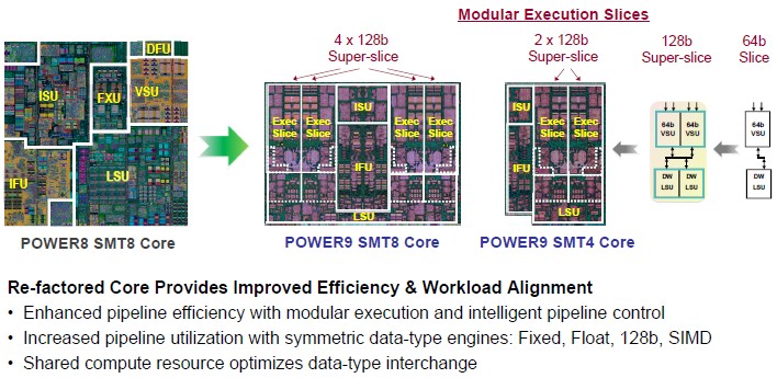
There was another form, vertical microprogramming, which was closer to RISC. But there was no translation from complex to vertical.
[1] https://www.cs.princeton.edu/courses/archive/fall10/cos375/B...
[2] https://inst.eecs.berkeley.edu/~n252/paper/RISC-patterson.pd...