The A510 small core is really the big news here for me. ARM updates their small core architecture very infrequently and the small cores hold back the features of their big cores. Because of the Cortex A55, the Cortex X1 was stuck on ARMv8.2. The OS needs to be able to schedule a thread on both small and big cores, you see. And that meant ARM’s own IP missed out on security features such as pointer authentication and memory tagging, which ARM customer Apple has been shipping for years at this point.
The Cortex A55 (announced 2017) was also a very minor upgrade over the Cortex A53 (announced 2012). These small cores are truly the baseline performance of application processors in global society, powering cheap smartphones, $30 TV boxes, most IoT applications doing non-trivial general computation and educational systems like the Raspberry Pi 3. If ARM’s numbers are near the truth (real-world implementations do like to disappoint us in practice), we’re going to see a nice security and performance uplift there. Things have been stale there a while.
If anything this announcement means that in a few years time, the vast majority of application processors sold will have robust mitigations against many important classes of memory corruption exploits [1].
I think especially the cheap smartphone space will benefit. Cheap Android phones are frequently so slow, they could use some cheap higher performance CPUs.
> Good phones are getting cheap. Cheap phones are getting good. -Someone who is not me
Marques Brownlee aka MKBHD and even he admitted that's not the case anymore.
Good phones are getting more and more expensive. A flagship used to cost $700 5 years ago, now it's $1000+.
Cheap phones are getting good, but not at the rate that good phones are getting more expensive.
> For what it's worth I'm still daily driving LG G2 and it's legit still fast, sure sometimes it's a bit sleepy but it's still more then usable!
A quick Googling tells me your phone is from 2013 and can only be updated to Android 5. Your phone is either:
* horrendously out of date and insecure
* using a custom ROM (which I, for one, and many others probably too, don't want to do)
* not used for any kind of internet facing activity (another thing that I and others don't want to do)
Also, you probably have a very low bar for usability and speed. With modern OSes and sites, that phone would probably be extremely slow and laggy for my (and many others') usage.
Your phone uses a Snapdragon 800 which probably has 10-15% (maybe 20-25% if I'm being generous) of the performance of a modern Snapdragon. Phones are not desktops/laptops, where performance levels plateaued in 2005.
I heard it from MKBHD too, but I wasn't sure if he was the original source :P
I wonder how much the inflation affected the pricing of the phones.
Also you can get Poco Phone or OnePlus Nord for reasonable amount of money. But your are right that I'm not the average user since my SIM card is in a Nokia 105, purely because of the battery life.
LG G2 is running a custom ROM with Android 9. And it honestly is usable. Gmail, MS Teams, Puzzle and Dragon, Dualingo and many more applications work without a problem. The probably major difference between how I use the phone and others would probably be that I don't leave applications running in the background. Probably because I think that RAM is the limiting factor here and not the CPU.
I think people don't realise how powerful modern phones actually are, I mean you can record and edit 4k video on today's flagship phones and probably much more.
(ps: yes I carry two phones with me, although I do quite often leave the smart one at home, since the Nokia can handle calls and messages without a problem)
Interesting note, for a 8 years old phone the battery still lasts me the whole day!
I will shed a small tear for the passing of AArch32 as it was the first processor architecture I really enjoyed programming.
I wrote hundreds of thousands of lines of assembler for it and what a fun architecture it was to program for. Enough registers to mean you rarely needed extra storage in a function and conditional instructions to lose those branches and combine that with 3 register arguments to each instruction meant that there was lots of opportunity for optimisation. Plus the (not very RISC but extremely useful) load and store multiple instructions and that made it a joy to work with.
AArch64 is quite nice too but they took a some of the fun out of the instruction set - conditional execution and load and store multiple. They did that for good reason though in order to make faster superscalar processors so I don't blame them!
Also fun bits for optimization: the barrel shifter that can be used on the second argument in any instruction, and the possibility to make any instruction conditional on the flags.
...At some point I started an x86 on Arm emulator, and managed to run x86 instructions in like 5-7 Arm instructions, without JIT, including reading next instruction and jumping to it - all thanks to the powerful Arm instruction set.
I was going to make a snarky comment about how all CPU architectures die, but it's not so easy to find a major one that isn't still used somewhere by someone—either in its original form or a distant derivation of it. Whether it's the Zilog Z80 or the Motorola 68000 series, there's probably still someone still actively using them embedded into cheap devices, or industrial computing, or automotive parts, or in military systems, or rad-hardened aerospace.
Fun story: Pachinko, Japanese gamble machine like Slot, is still enforced to use Z80 for calculating winning chance, to be able to regulator could check the calculating logic.
I've never played them but I heard something like: Throwing metal ball is completely physical, but if a ball fell into a specific pocket (at maybe specific timing or order?), computer determines is it win or not. If it decided to win, then special mode starts and possibly earn more metal balls.
At least in the M0 range, A64 won't be competitive on a gate count basis. M0s can be ridiculously tiny, down to ~12k gates, which is how they were able to take a huge chunk out of the market that had previously been 8/16 bit processors like 8051s and the like.
Power consumption is a hard constraint. The benefits of A64 have to outweigh the cost in power consumption, and the benefits just aren't there. Coin cells, small solar collectors and supercaps are among the extremely limited power sources for many Cortex M applications.
Many reasons. Cost being the biggest (64bit dies would cost way more than the 32bit ones) and power consumption (having a complex pipeline with 64bit registers isn't great when you have to run on a coin cell for a year).
Similar reasons to why 8 and 16 bit micros stuck around for so long in low cost and low power devices before Cortex M0+ became cheap and frugal enough.
My current Cortex-M4 project is about 40kB of code, and it runs at 48MHz. If I needed more performance, would just get one with a higher clock-rate. 64-bit has zero advantages in this context.
Also, worth mentioning that our safety-critical auditor recommends staying on 90nm or larger chips. That’s many of the Cortex chips, and the same as the original iPhone.
> not very RISC but extremely useful.. load and store multiple
Who was it that said that R and RISC as a nomenclature was always hogwash. A more apt name would be “load-store architecture”
Onne random thing I remember about LDM/STM was the earliest rev silicon of the Motorola (now Freescale) ARM based DragonBall (then better named the MX line) was the ARM9 core had a bug where LDM/STM would not work with the cache enabled - which of course was horrible, so we hacked gcc to not emit these instructions as a temporary workaround.
I think everyone is blowing past the real story here.
A72 cores are 10% slower than A73 per clock.
A510 is also supposed to be around 10% slower than A73 -- about the same performance as A72.
The big difference is that A72 is out-of-order while A510 is in-order. This means that A510 won't be vulnerable to spectre, meltdown, or any of the dozens of related vulnerabilities that keep popping up.
For the first time, we can run untrusted code at A72 speeds (fast enough for most things) without worrying that it's stealing data.
In-order CPUs aren't automatically immune to speculative execution exploits. ARM's A8 core is an example of an in-order core that was vunable.
It's speculative execution that causes problems, and in-order CPUs still do speculative execution during branch prediction. It's just that they typically get through less instruction while speculating.
All you need for Spectre is a branch misperception that lasts long enough for a dependent load.
However, it's been over three years since ARM have known about Meltdown and Spectre. There is a good chance the A510 is explicitly designed to be resistant to those exploits.
Spectre is because computers are memory bound so branch prediction without being able to touch memory is useless, and touching memory is very hard to undo, not because of out of order execution as per se.
They do but almost no in order design can manage to load a value from memory and then launch another load from the location based on that value before the branch resolves and the speculation is aborted. IIRC the Cortex A8 and Power 6 are the only two in order processors vulnerable to Specter.
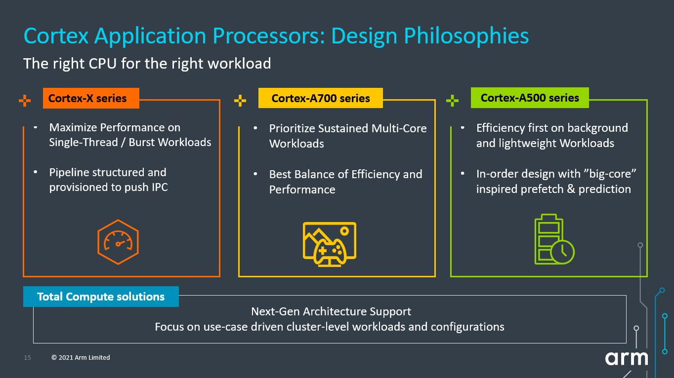
Interestly, I think they do (I don't know much about them). ARM's own infographic[0] says "In-order design with 'big-core' inspired prefetch & prediction", not sure if that's the same branch prediction we're talking about in regards to Spectre, etc.
Interesting that mobile platforms / CPU's losing 32 bit support whilst the dominant desktop platform retains it.
Not sure what the cost of continuing 32 bit support on x86 is for Intel/AMD but does there come a point when Intel/AMD/MS decide that it should be supported via (Rosetta like) emulation rather than in silicon?
My understanding is AArch64 is more or less fresh vs AArch32, whereas the ia16/ia32/amd64 transitions are all relatively simple extensions. Almost all the instructions work in all three modes, just the default registers are a bit different and the registers available are different and addressing modes might be a smidge different. You would make some gains in decoder logic by dropping the older stuff, but not a whole lot; amd64 still has the same variable width instructions and strong memory consistency model that make it hard.
If you dropped 16-bit and i386 then you might be able to reuse some of the shorter instruction codes like 0x62 (BOUND) that aren't supported in x86-64.
Decoders aren't the problem with variable length instructions anyway (and they can be good for performance because they're cache efficient.) The main problem is security because you can obfuscate programs by jumping into the middle of instructions.
The cost of continuing support is increased decoder complexity. The simplicity/orthogonality of the ARM ISA allows simpler instruction decoders. Simpler, faster, and easier to scale. Intel and AMD instruction decoders are impressive beasts that consume considerable manpower, chip space, and physical power.
I remember reading (in 2012 maybe) that ISA doesn't really matter and decoders don't really matter for performance. The decoder is such a small part of the power and area compared to the rest of the chip. I had a hypothesis that as we reach the tail end of microarchitectural performance the ISA will start to matter a lot more, since there are fewer and fewer places left to optimize.
Well now in 2021 cores are getting wider and wider to have any throughput improvement and power is a bigger concern than ever. Apple M1 has an 8-wide decoder feeding the rest of the extremely wide core. For comparison, Zen 3 has a 4-wide decoder and Ice Lake has 5-wide. We'll see in 3 years if Intel and AMD were just being economical or unimaginative or if they really can't go wider due to the x86 decode complexity. I suppose we'll never really know if they cover for a power hungry decoder with secret sauce elsewhere in the design.
The state-machine that can determine the start-of-instructions can be run in parallel. In fact, any RegEx / state machine / can be run in parallel on every byte with Kogge-stone / parallel prefix, because the state-machine itself is an associative (but not communitive) operation.
As such, I believe that decoders (even complicated ones like x86) scale at O(n) total work (aka power used) and O(log(n)) for depth (aka: clock cycles of latency).
-------
Obviously, a simpler ISA would allow for simpler decoding. But I don't think that decoders would scale poorly, even if you had to build a complicated parallel-execution engine to discover the start-of-instruction information.
I am not sure what you mean by running in parallel.
On x86, to be able to determine whether a given byte is the start of an instruction, the start of the part of an instruction following the variable-number of prefix bytes or another kind of byte, requires information from the decoding of the previous bytes.
So you may have as many pre-decoders as the fetched bytes, all starting decoding in parallel, but they are not independent and the later pre-decoders need the propagation of signals from the first pre-decoders, so the delay required for determining the initial instruction bytes grows with the number of bytes fetched and examined simultaneously (16 bytes for most x86 CPUs, which on average may contain 4 or 5 instructions).
We do not know for sure where the exact limitation is, but despite the vague and inconsistent information from the vendor documentation, which in a few cases seems to imply better capabilities, until now no Intel or AMD CPU has been shown to be able to decode more than 4 instructions simultaneously (the only exception is that some pairs of instruction are fused, e.g. some combinations of compare-and-branch, and those count as a single instruction for decoding, increasing the apparent number of simultaneously decoded instructions when those pairs occur in the program).
> I am not sure what you mean by running in parallel.
I literally mean in parallel. Computing a FSM from "backwards" and "forwards" simultaneously, as well as "from the middle outward". From all bits, simultaneously, in parallel.
As I stated earlier: Kogge-Stone carry save adder is the first step to understanding this.
Lets take 32-bits of two numbers: A[0:31] and B[0:31]. C [0:32] = A + B.
Simple, yes? Lets focus on purely a singular bit: C[32], the so called "carry bit". It is easy to see that the carry bit (the 33rd bit of the addition operation) depends on all 32-bits of A, as well as all 32-bits of B.
Nonetheless, the carry bit can be computed in parallel with Kogge-Stone (as well as other parallel carry-lookahead adders).
I've explained this process in multiple sibling posts at this point. Please give them a look first, and ask questions after you've read them. I understand that I've written quickly, verbosely, and perhaps inaccurately, but hopefully there's enough there to get started.
>because the state-machine itself is an associative (but not communitive) operation.
Proof?
> But I don't think that decoders would scale poorly, even if you had to build a complicated parallel-execution engine to discover the start-of-instruction information.
Surely we have empirical proof of that in that Apple's first iteration of a PC chip is noticeably wider than AMD's top of the line offering. On top of this we know that to make X86 run fast you have to include an entirely new layer of cache just to help the decoders out.
We've had this exact discussion on this site before, so I won't start it up again but even if you are right that you can decode in this manner I think empirically we know that the coefficient is not pretty.
I'm not a chip designer. I don't know the best decoding algorithms in the field.
What I can say is, I've come up with a decoding algorithm that's clearly O(n) total work and O(log(n)) depth. From there, additional work would be done to discover faster methodologies.
The importance of proving O(n) total work is not in "X should be done in this manner". Its in that "X has asymptotic complexity of at worst case, this value".
I presume that the actual chip designers making decoders are working on something better than what I came up with.
> Proof?
Its not an easy proof. But I think I've given enough information in sibling posts that you can figure it out yourself over the next hour if you really cared.
The Hillis / Steele paper is considered to be a good survey of parallel computing methodologies in the 1980s, and is a good read anyway.
One key idea that helped me figure it out, is that you can run FSM's "backwards". Consider a FSM where "abcd" is being matched. (No match == state 1. State 2 == a was matched. State 3 == a and b was matched. State 4 == abc was matched, State5 == abcd was matched).
You can see rather easily that FSM(a)(b)(c)(d), applied from left-to-right is the normal way FSMs work.
Reverse-FSM(d) == 4 if-and-only if the 4th character is d. Reverse-FSM(other-characters) == initial state in all other cases. Reverse-FSM(d)(c) == 3.
In contrast, we can also run the FSM in the standard forward approach. FSM(a)(b) == 3
Because FSM(a)(b) == 3, and Reverse-FSM(d)(c) == 3, the two states match up and we know that the final state was 5.
As such, we can run the FSM-backwards. By carefully crafting "reverse-FSM" and "forward-FSM" operations, we can run the finite-state-machine in any order.
Does that help understand the concept? The "later" FSM operations being applied on the later-characters are "backwards" operations (figuring out the transition from transitioning from state4 to state 3). While "earlier" FSM operations on the first characters are the traditional forward-stepping of the FSM.
When the FSM operations meet in the middle (aka: FSM(a)(b) meets with reverse-FSM(c)), all you do is compare states: reverse-FSM(c) declares a match if-and-only-if the state was 3. FSM(a)(b) clearly is in state 3, so you can combine the two values together and say that the final state was in fact 4.
-----
Last step: now that you think of forward and reverse FSMs, the "middle" FSMs are also similar. Consider FSM2(b), which processes the 2nd-character: the output is basically 1->3 if-and-only-if the 2nd character is b.
FSM(a) == 1 and ReverseFSM(d)(c) == 3, and we have the middle FSM2 returning (1->3). So we know that the two sides match up.
So we can see that all bytes: the first bytes, the last bytes, and even the middle bytes, can be processed in parallel.
For example, lets take FSM2(b)(c), and process the two middle bytes before we process the beginning or end. We see that the 2nd byte is (b), which means that FSM2(b)(c) creates a 2->4 link (if the state entering FSM2(b)(c) is 2, then the last state is 4).
Now we do FSM(a), and see that we are in state 2. FSM(a) puts us in state 2, and since FSM2(b)(c) has been preprocessed to be 2->4, that puts us at state 4.
So we can really process the FSM in any order. Kogge-Stone gives us a O(n) work + O(log(n)) parallel methodology. Done.
Its pretty obvious to me that the x86 prefix-extensions to the ISA are a Chomsky Type3 regular grammar. Which means that a (simple) RegEx can describe the x86 prefixes, which can be converted into a nondeterministic finite automata, which can be converted into a deterministic finite state machine.
Or under more colloquial terms: you "parse" a potential x86 instruction by "Starting with the left-most byte, read one-byte at a time until you get a complete instruction".
Any grammar that you parse one-byte-at-a-time from left-to-right is a Chomsky Type3 grammar. (In contrast: 5 + 3 * 2 cannot be parsed from left to right: 3*2 needs to be evaluated first before the 5+ part).
My point is that the ARM's ISA vs x86 ISA is not any kind of asymptotic difference in efficiency that grossly prevents scaling.
Even the simplest decoder on a exactly 32-bit ISA (like POWER9) with no frills would need O(n) scaling. If you do 16-instructions per clock tick, you need 16x individual decoders on every 4-bytes.
Sure, that delivers the results in O(1) instead of O(log(n)) like a Kogge-stone FSM would do, but ARM64 isn't exactly cake to decode either. There's microop / macro-op fusion going on in ARM64 (ex: AESE + AESMC are fused on ARM64 and executed as one uop).
> x86 instructions can straddle MMU pages and even cache lines.
That doesn't change the size or power-requirements of the decoder however. The die-size is related to the total-work done (aka: O(n) die area). And O(n) also describes the power requirements.
If the core is stalled on MMU pages / cache line stalls, then the core idles and uses less power. The die-area used doesn't change (because once fabricated in lithography, the hardware can't change)
> (assuming that’s true. I wouldn’t even dare say I believe that or its converse)
The original application was the Kogge-stone carry-lookahead adders. How do you calculate the "carry bit" in O(log(n)) time, where n is the number of bits? It is clear that a carry bit depends on all 32-bits + 32-bits (!!!), so it almost defies logic to think that you can figure it out in O(log(n)) depth.
You need to think about it a bit, but it definitely works, and is a thing taught in computer architecture classes for computer engineers.
--------
Anyway, if you understand how Kogge-Stone carry lookahead works, then you understand that any associative operation (of which "Carry-bit" calculations is associative). The next step is realizing that "stepping a state machine" is associative.
There, Hillis / Steel prove that FSM / regex parsing is an associative operation, and therefore can be implemented in the Kogge-stone adder (called a "prefix-sum" or "Scan" operation in that paper).
You're right about the implications of Kogge-Stone, but constant factors matter a lot.
In fixed width ISAs, you have N decoders and all their work is useful.
In byte granularity dynamic width ISAs, you have one (partial) decoder per byte of your instruction window. All but N of their decode results are effectively thrown away.
That's very wasteful.
The only way out I can see is if determining instruction length is extremely cheap. That doesn't really describe x86 though.
The other aspect is that if you want to keep things cheap, all this logic is bound to add at least one pipeline stage (because you keep it cheap by splitting instruction decode into a first partial decode that determines instruction length followed by a full decode in the next stage). Making your pipeline ~10% longer is a big drag on performance.
> In fixed width ISAs, you have N decoders and all their work is useful.
ARM isn't fixed width anymore. AESE + AESMC macro-op fuse into a singular opcode, for example.
IIRC, high performance ARM cores are macro-op fusing and/or splitting up opcodes into micro-ops. Its not necessarily a 1-to-1 translation from instructions to opcodes anymore for ARM.
But yes, a simpler ISA will have a simpler decoder. But a lot of people seem to think its a huge, possibly asymptoticly huge, advantage.
-----------------
> The only way out I can see is if determining instruction length is extremely cheap. That doesn't really describe x86 though.
I just described a O(n) work / O(log(n)) latency way of determining instruction length.
Proposal: 1. have a "instruction length decoder" on every byte coming in. Because this ONLY determines instruction length and is decidedly not a full decoder, its much cheaper than a real decoder.
2. Once the "instruction length decoders" determine the start-of-instructions, have 4 to 8 complete decoders read instructions starting "magically" in the right spots.
That's the key for my proposal. Sure, the Kogge-stone part is a bit more costly, but focus purely on instruction length and you're pretty much set to have a cheap and simple "full decoder" down the line.
You're right in a sense, in that even really hairy decode problems like x86 only add 15% or so to a core's overall power usage.
But on the other hand verification is a big NRE cost for chips and proving that that second ISA works correctly in all cases is a pretty substantial engineering cost even if the resulting chip is much the same.
It likely wouldn't be 15% with an 8-wide x86 decoder if such a thing would even be possible within any reasonable clock budget. So in that sense a fixed width ISA does buy something. Also, given that chips today are mostly power limited, 15% power usage is 15% that could be used to increase performance in other ways.
> The simplicity/orthogonality of the ARM ISA allows simpler instruction decoders. Simpler, faster, and easier to scale. Intel and AMD instruction decoders are impressive beasts that consume considerable manpower, chip space, and physical power
These claims are often made and indeed make some sense but is there any actual evidence for them? To really know you'd need access to the RTL of both cutting edge x86 and arm designs to do the analysis to work out what the decoders are actually costing in terms of power and area and whether they tend to produce critical timing paths. You'd also need access to the companies project planning/timesheets to get an estimate of engineering effort for both (and chances are data isn't really tracked at that level of granularity, you'll also need a deep dive of their bug tracking to determine what is decoder related for instance and estimate how much time has been spent on dealing with decoder issues). I suspect Intel/AMD/arm have no interest in making the relevant information publicly available.
You could attempt this analysis without access to RTL but isolating the power cost of the decoder with the silicon alone sounds hard and potentially infeasible.
x86 die breakdowns put the area of the decoder as bigger than the integer ALUs. While unused ALUs can power gate, there's almost never a time when the decoders are not in use.
Likewise, parsing is a well-studied field and parallel parsing has been a huge focus for decades now. If you look around, you can find papers and patents around decoding highly serialized instruction sets (aka x86). The speedups over a naive implementation are huge, but come at the cost of many transistors while still not being as efficient or scalable as parallel parsing of fixed-length instructions. The insistence that parsing compressed, serial streams can be done for free mystifies me.
I believe you can still find where some AMD exec said that they weren't going wider than 4 decoders because the power/performance ratio became much too bad. If decoders weren't a significant cost to their designs (both in transistors and power), you'd expect widening to be a non-issue.
I'm sure that Arm must have done a lot of analysis around this issue when AArch64 was being developed.
After all the relatively simple Thumb extension had been part of the Arm ISA for a long time (and was arguably one of the reasons for its success) and they still decided to go for fixed width.
Also out of interest do you have a link to an x86 die breakdown that includes decoder and ALU area? Looking at wikichip for example they've got a breakdown for Ice Lake: https://en.wikichip.org/wiki/intel/microarchitectures/ice_la... but it doesn't get into that level of detail, a vague 'Execution units' that isn't even given bounds is the best you get and is likely an educated guess rather than definite knowledge of what that bit of die contains. Reverse engineering from die shots can do impressive things but certainly what you see in public never seems to get into that level of detail and would likely be significant effort without assistance from Intel.
Here you go. This one combines a high-res die shot with AMD's die breakdown of Zen 2.
You'll notice that I understated things significantly. Not only is decoder bigger than the integer ALUs, but it's more than 2x as big if you don't include the uop cache and around 3x as big if you do! It dwarfs almost every other part of the die except caches and the beast that is load/store
Thanks, my mistake was searching exclusively for Intel micro-architecture. It'd be interesting to see if there are further similar die breakdowns for other micro-architectures around, trawling through conference proceedings likely to yield better results than a quick Google. Just skimming through hot chips as it has a publicly accessible archive (those AMD die breakdowns come from ISSCC which isn't so easily accessible).
The decoder is certainly a reasonable fraction of the core area, though as a fraction of total chip area it's still not too much as other units in core are of similar size or larger size (Floating point/SIMD, branch prediction, load/store, L2) plus all of the uncore stuff (L3 in particular). Really we need a similar die shot of a big arm core to compare its decoder size too. Hotchips 2019 has a highlighted die plot of an N1 with different blocks coloured but sadly it doesn't provide a key as to which block is what colour.
I guess I'm making the wrong argument. I'd agree it's clear an x86 decoder will be bigger, more power hungry etc than an arm decoder. The real question is how much of a factor that is for the rest of the micro-architecture? Is the decoder dragging everything down or just a pain you can deal with at some extra bit of power/area cost that doesn't really matter? That's what I was aiming to get at in the call for evidence. Is x86 inherently inferior to arm and cannot scale as well for large super scalar CPUs because the decoder drags you down or is Apple just better at micro-architecture design (perhaps AMD's team would also fail to scale well beyond 4 wide with an arm design, perhaps Apple's team could have built an x86 M1).
As I understand it, the fact that x86 has variable-length instructions makes a significant difference. On ARM if you want to look ahead to see what the next instructions are, you can just add a fixed offset to the address of the current instruction. If you want to do that on x86, you have to do at least enough work to figure out what each instruction is, so that you know how large it is, and only then will you know where the next instruction begins. Obviously this is not very amenable to any kind of concurrent processing.
You can do quite a bit concurrently, but at the expense of hardware. You ‘just’ speculatively assume an instruction starts at every byte offset and start decoding.
Then, once you figure out that the instruction at offset 0 is N bytes, ignore the speculative decodings starting at offsets 1 through N-1, and tell the speculative decoding at offset N that it is good to go. That means that it in turn can inform its successors whether they are doing needless work or are good to go, etc.
That effectively means you need more decoders, and, I guess, have to accept a (¿slightly?) longer delay in decoding instructions that are ‘later’ in this cascade.
> the cost of continuing 32 bit support on x86 is for Intel/AMD
Pretty sure they still have 16-bit support.
It's easier to migrate for a CPU mostly used for Android because it's already had a mix of architectures, there are fewer legacy business applications, and distribution through an app store hides potential confusion from users.
Another advantage the Android platform has specifically is that its applications mostly consist of bytecode, limiting the impact phasing out 32 bit instructions has on the platform. Most high performance chips are in Android devices like phones and tablets where native libraries are more the exception than the rule.
Desktop relies on a lot of legacy support because even today developers make (unjust) assumptions that a certain system quirk will work for the next few years. There's no good reason to drop x86 support and there's good reason to keep it. The PC world can't afford to pull an Apple because there's less of a fan cult around most PC products that helps shift the blame on developers when their favourite games stop working.
Run-anywhere was (and halfway still is) a huge selling point for Java. It was always clunky for desktop apps because of slow JVM warmup and nothing feeling native, but Android shifted enough of that into the OS so it's not a problem.
I suppose idly wondering at what point the legacy business applications become so old that the speed penalty of emulation becomes something that almost everyone can live with.
>We’ve seen that Samsung’s 5LPE node used by Qualcomm and S.LSI in the Snapdragon 888 and Exynos 2100 has under-delivered in terms of performance and power efficiency, and I generally consider both big cores' power consumption to be at a higher bound limit when it comes to thermals.
I expect Qualcomm to stick with Samsung foundry in the next generation, so I am admittedly pessimistic in regards to power improvements in whichever node the next flagship SoCs come in (be it 5LPP or 4LPP). It could well be plausible that we wouldn’t see the full +16% improvement in actual SoCs next year.
Honestly, they're probably stuck with Samsung for the mid term (5 years). You simply can't get any TSMC capacity on their top nodes when Apple and AMD get first and second bid on everything. Maybe GloFo will figure out their issues, and maybe Intel will sell their latest nodes, but until then companies are stuck with their current partners.
Didn't gloflo officially announce they will stick to >14nm a few years ago? Have they started developing a new node? IIRC they just didn't have the capital to keep churning out a few dozens of billions on r&d/equipment every few years, so they shifted their focus on maximizing yield on older nodes
Could anyone explain the main differences between this new Armv9 CPU and the Apple M1 ARMs? What are the strengths and weaknesses of the two or is one lightyears ahead of the other?
ARMv8 is a big target [0]. You have 6 major ISA extensions of which recent ARM designs support 2 and Apple's support 5. There's also SVE which was a kind of side-option. In addition, there's the 32-bit version, the 64-bit version, the R and A versions all with different capabilities and support levels.
ARMv9 tries to unify that a bit [1]. They add a new security model and SVE moves from a side option to a requirement. A bunch of the various v8 instructions also get bundled into the core requirements.
A14 vs X2 is a different question. A14/M1 really dropped the ball by not supporting SVE. I suspect they will support it in their next generation of processors, but the problem is adoption. Everyone is jumping on the M1 units and won't be upgrading their laptops for another few years. As such, they'll be held back for the foreseeable future.
Performance is no question and A14 will be retaining its lead for the next 2-3 years at least. X1 chips are already significantly slower than A14 chips. X2 only increases performance by 10-16% (as pointed out in the article, the 16% is a bit disingenuous as it compares X1 with 4mb cache to the x2 with 8mb of cache while X1 gets a decent speedup with the 8mb version). Furthermore, by the time X2 is actually in devices, Apple will already be launching their own next generation of processors (though I suspect we're about to see them move to small performance increases due to diminishing returns).
A14 is 3.1GHz while A13 is 2.66GHz. A14 is around 20% faster than A13 overall, but it is also clocked 14% higher which gives only around 6% more IPC. Power consumption all but guarantees that they won't be doing that too often.
Where does the A14/M1 suffer due to the lack of SVE? The performance of M1 is well known to be terrific, so it’s hard to characterize that as dropping the ball in my book. More like they prioritized other features instead, and they ended up creating a great processor.
I suppose they "dropped the ball" in the sense that those instructions cannot be assumed to be available, thus will not be encoded by the compiler by default. Any future processors which include the instructions may not benefit until developers recompile for the new instructions and go through the extra work required to conditionally execute when available.
That said, to get the best performance on vector math it has long been recommended to use Apple's own Accelerate.framework, which has the benefit of enabling use of their proprietary matrix math coprocessor. One can expect the framework to always take maximum advantage of the hardware wherever it runs with no extra development effort required.
* only use NEON to save developer time and lose performance and forward compatibility
* only use SVE to save developer time and lose backward compatibility
* Pay to support both and deal with the cost/headaches
Experience shows that AVX took years to adopt (and still isn't used for everything) because SSE2 was "good enough" and the extra costs and loss of backward compatibility weren't worth it.
If SVE were supported out of the gate, then the problem would simply never exist. Don't forget (as stated before) that there's been a huge wave of M1 buyers. People upgraded early either to get the nice features or not be left behind as Apple drops support.
Let's say you have 100M Mac users and an average of 20M are buying new machines any given year (a new machine every 5 years). The 1.5-2-year M1 wave gets 60-70M upgraders in the surge. Now sales are going to decline for a while as the remaining people stick to their update schedule (or hold on to their x86 machines until they die). Now the M2 with SVE only gets 5-10M upgraders. Does it make sense to target such a small group or wait a few years? I suspect there will be a lot of waiting.
SVE vs NEON performance will also hugely depend on the vector length the given algorithm requires, and the stress that the instructions put on the memory subsystem.
Memory hierarchy varies by product and will likely continue to do so regardless of what M2 does.
In the end, I echo eyesee's comment, for best performance one should really use Accelerate.framework on Apple's hardware.
My point was that it probably doesn’t matter. M1 is already very fast, even without SVE. At some point you just have to decide to ship a product, even if it doesn’t have every possible feature.
Like other posters mentioned, for vector operations like this, you could be dynamically linking to a library that handles this for you in the best way for the hardware. Then when new instructions become available, you don't have to change any of your code to take advantage.
The Arm X2 is still going to be behind Apple Firestorm but at least Arm won't be trailing by 50% any more. At least for now Arm doesn't have an appetite for create monster 8-issue cores.
> In terms of the performance and power curve, the new X2 core extends itself ahead of the X1 curve in both metrics. The +16% performance figure in terms of the peak performance points, though it does come at a cost of higher power consumption.
If you read on a bit, there is some question that those performance metrics will be seen in the real world, due to existing thermal issues.
> I am admittedly pessimistic in regards to power improvements in whichever node the next flagship SoCs come in (be it 5LPP or 4LPP). It could well be plausible that we wouldn’t see the full +16% improvement in actual SoCs next year.
In general for moving from v8 to v9, I think 16% is extremely pessimistic.
Removal of aarch32 has huge implications. And this is not limited to CPU but also touches MMU, caches and more that in v8 had to provide aarch32 compatible interfaces. This lead to really inefficient designs (for example, MMU walk which is extremely critical to performance is more than twice as complicated in ARMv8 compared to v7 and v9).
The space saved by removing these can be used for bigger caches, wider units, better branch prediction and other fun stuff.
Finally, note also that the baseline X1 numbers come from Samsung who we all know are worst in class right now. And they are using an inferior process. Let's see what qcomm, ampere and amazon can do with v9.
Does Apple's M1 still support AArch32, it using an ARMv8.4-A instruction set ? I'm assuming no 32-bit code is ever executed on macOS on ARM, how much die space would removing the 32-bit support save ?
With WWDC '21 being only weeks away, I wonder if we're going to see an ARMv9 M2.
AFAIK none of the (current) apple produced processors do 32 bit, even the apple watch. Which is interesting, as it is very memory constrained, the usual reason for using 32 bit code.
Judging by some LLVM patches by an apple engineer, they solved this by creating an ILP32 mode for Aarch64 where they use the full 64 bit mode but with 32 bit pointers.
No. There is no AArch32 on the M1. Even things like the A32 relevant bits in the Apple-proprietary performance counters are reserved and unimplemented.
iOS 11 was the first Apple OS to not run 32-bit apps so I'm guessing the iPhone X that was released later that year (2017) with the A11 Bionic chip was the first to drop 32-bit support.
Perhaps more relevant to the M1, though, is that OS X dropped support for 32-bit apps about 18 months back, with Catalina. The timing there seems just too coincidental to not have been done in order to pave the way for the M1.
Indeed. I think throwing out 32 bit support in Catalina was in preparation for the M1 one year later. Not so much because the M1 is 64 bit only, as 32 bit x86 applications wouldn't have run on it either way. Perhaps to make Rosetta simpler, as it only had to support 64 bit code.
But also with Catalina, all old and unmaintained applications did no longer run. Those applications, which run on Catalina, do run on M1. Which made the switch from x86 to ARM cpus much smoother for the users. The hard cut had been done with Catalina already - and this is the reason my private Mac still runs Mojave :p. When I get a new Mac, switching to ARM doesn't create any less backwards compatibility than switching to Catalina would...
Rosetta supports translating 32-bit x86 instructions. However, there are no native 32-bit OS libs anymore.
This means that you have to do the thunking back and forth yourself to call OS libraries. The only x86 program using this facility so far is Wine/CrossOver on Apple Silicon Macs, which as such runs 32-bit x86 apps...
I want to emphasize it's unknown whether this is the successor to the M1 by major or minor version - but it's more likely that this is a production ramp-up for the new Pro machines to be announced during WWDC and will likely ship later this summer.
The successor to the M1, the lowest-end Apple Silicon running on Macs, is likely expected next year in a rumored redesign of the Macbook Air (whatever the CPU itself is called)
This is what I am banking on. I want to get another year out of my old Intel Macs before getting an MX-based Macbook that should melt my eyeballs with its speed while lasting a day and a half on battery.
M1 is Armv8.5-A, which is almost the same as Armv9.0-A, except that it lacks SVE2 vector instructions. Apple's CPUs tend to move to the latest architecture revision that is available at the time the instruction set gets nailed down, so the next generation (M2 and A15) would be Armv8.6-A if it lacks SVE2, or Armv9.1-A if it includes it.
Most likely the M2/A15 will include SVE2 but won't be available for another six months, while the M1+ in the coming Macbook Pro would still be Armv8.5-A.
I find the clustering approach in A510 very intriguing.
Why run the low power cores in pair? Is this because android _really_ struggles on single core due to the way it was designed? So you basically need two cores even when mostly idle?
The two cores only share FP and vector execution units. A ton of code doesn't use those at all, and so they are effectively two separate cores most of the time. It provides full compatibility on both cores, full performance very often, and saves a lot of die area (FP and vector are going to be very transistor-heavy). It's just a tradeoff.
This is actually worse than I thought compared to N2 used on Server. N2 was suppose to have 40% IPC increase, comparatively speaking.
> In terms of the performance and power curve, the new X2 core extends itself ahead of the X1 curve in both metrics. The +16% performance figure in terms of the peak performance points, though it does come at a cost of higher power consumption.
The 16% figure was done with an 8MB Cache compared to a 4MB Cache on X1. i.e In the absolute ( also unrealistic ) best case scenario, with an extra 10% Clock-speed increase, you are looking at single core performance of X2, released with flagship phone in 2022, to be roughly equivalent to A13 used on iPhone 11, released in 2019.
The most interesting part is actually the LITTLE Core A510. I am wondering what it would bring to low cost computing. Unfortunately no Die Size estimate were given.
Not directly related to these new fancy cores, but I was looking at the product range and noticed Cortex-A34 core in there that has snuck by quietly. I couldn't find any hardware, chips or devices, that are using that core. It has the interesting property that its AArch64 only, like these new ones. Has anyone seen or heard about it in the wild?
TLDR seems to be that next year's Cortex X2 and A710 are very incremental upgrades (+10-15%) over existing, at least compared to what ARM has delivered in the recent years. The A510 seems promising for the little core. Wait for the 2023 next gen Sophia-based designs if you can.
Given the industry's reliance on ARM's CPU designs, I wonder if it makes sense for prosumers / enthusiasts to keep track of these ARM microarchitectures instead of, say, Qualcomm Snapdragon 888 and Samsung Exynous 2100. Because ultimately the ARM architecture is the cornerstone of performance metrics in any non-Apple smartphone.
Conversely, it'll be interesting to see how smartphone OEMs market their 2022 flagship devices when it's clearly insinuated that the CPU performance on the next-gen ARM cores will not be much of an uplift compared to current gen. Probably more emphasis on camera, display and design.
"The immediate goals for the NUVIA team will be implementing custom CPU cores into laptop-class Snapdragon SoCs running Windows" - Qualcomm’s Keith Kressin, SVP and GM, Edge Cloud and Computing
I thought Nuvia's designs are for higher TDP products like laptops and servers, rather than mobile SOCs. But it'd make sense for both segments, e.g. scaling core count.
Why did ARM have to abandon their nice, clean numbering system of basically just increasing the number in each family by one, and go for just completely random meaningless numbers that jump by an order of magnitude for no reason... Such a waste of a clean and understandable lineup.
> The new CPU family marks one of the largest architectural jumps we’ve had in years, as the company is now baselining all three new CPU IPs on Armv9.0.
I believe the deprecation of AArch32 is quite an important change and by itself already warrants issuing a new major version (then there's all mandatory extensions from v8.2+ and SVE2).
They have not claimed to bump the major version on a regular basis from now as you seem to suggest.
That's a reasonable perspective to take. But the A710 still supports AArch32. And they were really close to a traditional re-vamp point anyways =P. This release (of the middle core) would have been then A79. The next release (the one that would actually deprecate AAarch32) would have been A80... and doing weird shit when you reach "10" would just follow in the grand tradition of tech. I think really only Intels somehow just... kept counting up in a more or less sane way.
It'd be interesting to know the thought process behind their terrible naming convention. From the outside, it looks like they went out of their way to making it as confusing as possible.
The Cortex A55 (announced 2017) was also a very minor upgrade over the Cortex A53 (announced 2012). These small cores are truly the baseline performance of application processors in global society, powering cheap smartphones, $30 TV boxes, most IoT applications doing non-trivial general computation and educational systems like the Raspberry Pi 3. If ARM’s numbers are near the truth (real-world implementations do like to disappoint us in practice), we’re going to see a nice security and performance uplift there. Things have been stale there a while.
If anything this announcement means that in a few years time, the vast majority of application processors sold will have robust mitigations against many important classes of memory corruption exploits [1].
[1]: https://googleprojectzero.blogspot.com/2019/02/examining-poi...