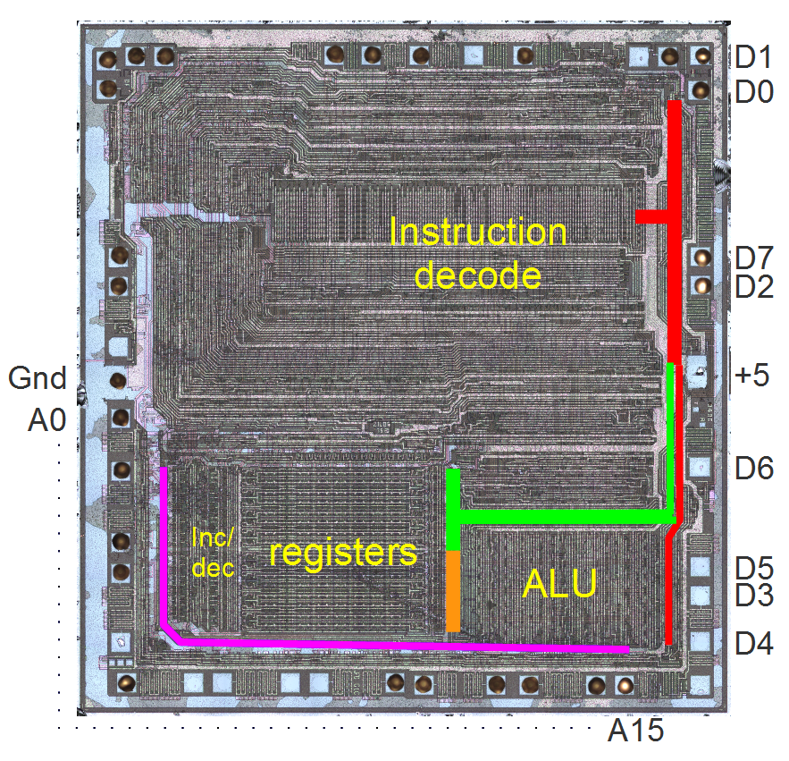
The 6502 has a PLA, as do many other early microprocessors such as the 6800, 8080, and Z-80. The PLA is a structured arrangement of logic gates, rather than a microcode ROM. But they both have a similar grid-like appearance.
Of course you're the expert here, but isn't this a little nitpicking? The decode logic of the Z80 (from your site[1]) works in much the same way as microcode by stepping through a set of fixed "instructions".
> Of course you're the expert here, but isn't this a little nitpicking?
No, a PLA [1] and a microcode ROM are two very different animals.
A PLA is a way of compactly specifying combinatorial logic circuits (arrangements of and/or/etc. gates) and in the form that gave it the name, it is end user programmable (the P stands for Programmable). But at its heart, a PLA is just a big arrangement of logic gates. A signal goes in, and after the necessary gate delays settle, the result signal comes out.
Microcode is literally a "program" and is 'executed' in the same way that all other programs are executed, one instruction at a time, addressed by a program counter. There are also often branching instructions that generate new program counter values to use to sequence through the various steps. None of which exists in a PLA.
The appearance of similarity arises because both look similar in a silicon die photo (rows and columns of transistors), but they are very different and perform quite different functions on the chip.
A consequence of this is the so-called "undocumented" opcodes of the 6502. Extra instructions such as LAX (load A and X from the same value) "work" because the instruction activates two different blobs of logic (the one for LDA plus the one for LDX). From my experience, it's less clear that microcode would function this way when confronted with an illegal opcode.
The PLAs on the Z80 and 6502 aren't user programmable, but had their functions fixed in the mask just like regular logic or a mask ROM would be.
Talking about the PLAs in these processors versus ucode ROM, the big difference is that in a PLA, typically several lines are enabled at a time. In contrast a ROM will only have one line active at a time with an address decoder sitting in front of it.
You absolutely could use a microcode ROM in the place of how these chips use their PLAs, it'd just take more die area.
You can see this logic/data equivalence in other places of hardware design too. For instance how FPGAs are a sea of SRAM, but are equivalent to standard cell chips. FPGAs are just slower, larger, and easier to modify.
> The PLAs on the Z80 and 6502 aren't user programmable,
I never said they were.
I said: "and in the form that gave it the name, it is end user programmable (the P stands for Programmable)" which is in the context of generic PLA's, not the specific PLA in a Z80 or 6502.
The difference is less clearcut than you're assuming. A PLA and a ROM are both types of lookup tables, after all, and in this application they're both being used to control the next state of a FSM.
> No, a PLA [1] and a microcode ROM are two very different animals.
Technically a microcode ROM (or any ROM, really) is a (degenerate case of a) PLA. Hence the visual similarities, since that type of grid pattern will be observed with any PLA, whether ROM or general-logic.
I suspect that at the time microcode was copyrightable while masks (and therefore PLAs) were not (note the actual (C) message on the die explicitly calling out the microcode)
Protection for "mask works" was introduced in the Semiconductor Chip Protection act of 1984. You'll see a circled-M on modern dies indicating this protection. (I got the mask work symbol added to Unicode recently, but font support is lacking: 🆭.) The 8086 is the only chip I've seen with a copyright specifically designating the microcode.
In the context of IC chip layouts, the determining factor is almost always die area. Some functions will be smaller on the die in PLA form, other functions will be smaller on the die in microcode form. Since die area is almost always a scarce resource, the chip designer will usually pick the design that reduces die area consumption for any given function.
(puts on chip designer hat) yes and no, as I said upstream the copyright laws of the time did not protect designs, chip copying (stealing) was rampant.
I can imagine that some CPU designers from a particular world view (especially in the 70s) might only design in terms of microcode - but also design tools were pretty minimal, I can imagine that it might have been far easier to design things in terms of microcode rather than as PLAs - what you might be seeing here is the differences between different teams' in house custom tooling
Not yet, but with these new high-resolution die photos it is only a matter of time.
Meanwhile the US4449184 patent [1] referenced in the post's footnotes has a lot of information about how the microcode works (and the meaning of the 21 instruction bits) and, in Tables 7-12, shows the microcode listings for some of the microcoded 8086 instructions.
probably not, but the data from this project should make that pretty easy
However to be useful you need to know what each of those 21-bits is connected to, some will essentially be risc-like uCode instructions, the others will be tied to particular functions in the CPU or memory interface
The Z-80 has an interesting way of executing instructions, but it's different from microcode. The first step is the PLA, which basically pattern-matches instructions into related categories, e.g. generating a signal for bit pattern 01XX100X, which might be instructions that read a value from the accumulator for instance.
There are two ways this is different from microcode. First, one instruction can trigger multiple "categories". Second, time is not an input here, so there is no stepping through operations.
The next part of the Z-80 instruction decoding is a big pile of AND-OR gates that generate the control signals based on the PLA outputs and the timing signals. For example, a gate might trigger the read-from-A-register signal for PLA-output-1 and time-1 or PLA-output-3 and time-1 or PLA output-1 and time-4. (These gates are all complex and were hand-drawn.)
The point of this is that both microcode and discrete logic generate particular control signals based on the instruction and time step, but they use very different ways to do this. With microcode, you can point to each micro-instruction as it executed, but in the Z-80, things are happening all over the place seemingly randomly.
I've always wondered why that is, given the space-constraints that affected the other areas of those parts' architecture. I assume it was just for development speed, given that the array was easier to lay out (and maybe even had some kind of primitive EDA tooling)?
A PLA is reasonably space-efficient if you need gates with a fixed set of inputs and outputs. Even the 8008 used one for instruction decoding. In addition to the microcode ROM, the 8086 has several PLAs of various sizes. For instance, one PLA converts the ALU operation into the necessary ALU control lines.
A key distinction is that in a ROM, only one row is active at a time. But in a PLA, multiple rows can be active simultaneously.(This is from "The Architecture of Microprocessors".)
Hmm, the top part of the die shot looks like microcode to me:
http://visual6502.org/images/6502/6502_top_op10x_BF_4677.png