I saw a video doing something like awhile ago [1], and I thought the idea of using electroplating made sense, but I know absolutely nothing about chemical engineering or material science.
It's interesting to see this idea in action, though with my limited experience with electroplating it seems like it'd be absurdly slow.
You're right - electroplating isn't traditionally very fast. Much of the system has been engineered to drive a build speed that's relevant for mass manufacturing while maintaining material properties (think 100-1000x faster than typical electroplating)
Very, very cool. If you can make metal 3D printing viable for consumers I'll be the first in line to buy one (though I realize that's probably quite a ways away).
I was interested in electrochemical 3D printing awhile back:
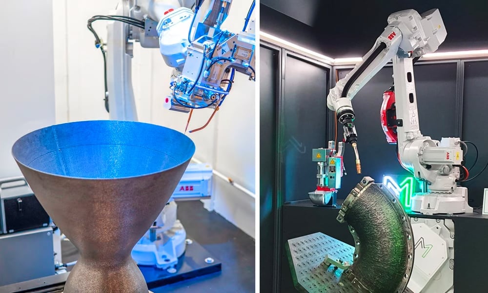
1. Deposition can be very precise (they say micron-level resolution here), but it's typically slow for a naive approach. That's not necessarily a problem if you need that precision. They say their approach is fast, probably by using some kind of array of nozzles (think an inkjet printer head).
2. You can also selectively run the process in reverse, so an electrochemical printer is actually a combo additive and subtractive manufacturing machine.
3. Because it's electrochemistry, I believe such a 3D printer is mostly restricted to depositing pure elemental metals and only a few alloys. This severely restricts your material selections.
Very cool to see this commercialized though, I'm curious how far they can take it.
> by using some kind of array of nozzles (think an inkjet printer head).
By bet is on electrospray ionization nozzles. It's a well understood technique thanks to mass spectrometers, it's just a matter of time before someone miniaturizes them and creates a way to control the spray pattern.
CTO of Fabric8 here - happy to answer any questions you may have about the technology or company. As you can tell we've got a process that's quite different than other metal AM techniques with some very unique benefits that we're excited to share!
Tons of questions, this is incredibly cool! Can you discuss:
1.) How you compensate for anode consumption/geometry changes over the lifetime of the anode. For instance, does the center get worn away or do you try to uniformly use each "pixel".
2.) More details on anode "pixel" geometry and minimum feature size.
3.) Can you talk about the development process? Did you have in situ measurement, or post build analysis of the part and anode.
It’s really cool and I wish I had one of these machines. On the assumption that I couldn’t afford such a machine myself for DIY, it would be really cool to have a send-cut-send like service. It seems like the relatively gentle process and I assume predictable results with minimal post processing would lend itself to an high degree of automation. Perhaps a scale out manufacturing set up where the speed of an individual machine is less important than the throughput of having many machines.
There are a lot of little random things that I would design if I knew there was a capability to have it made at non-aerospace prices. Initially heatsinks, manifolds, heat exchangers, but possibly many random things depending on the pricing.
Sure, there is a huge gamut of prices from aerospace to just above material costs. On the expensive side I would use it judiciously, on the economical side I would use it for just about everything and so would many others. I do a bit of DIY and a large amount of the design work is to work around limitations of cheaper materials and cheaper processes. Most of what I make is onesie-twosie where the design costs dominate so I can afford to spend more on a more expensive materials and processes to cut back on the design. But it would be extra amazing if there was an economical high quality process that is suitable for prototyping and would also be amenable to cost competitive mass manufacturing. That would be absolutely world changing. If I could just list designs somewhere and customers have them printed on demand, either via Amazon or some drop-ship, I could recoup a lot of the design costs so I could spend more time designing things - maybe even make a career out of it. Instead of needing a whole factory to support the low cost manufacturing of a single part it could just be a design document sitting on a server somewhere.
I understand that it is not in Fabric8s interest to do this though, expensive machines are high margin and exclusivity is required to maintain a bit of a monopoly for their customers so that their customers can justify purchasing the expensive machines in the first place. If Fabric8 were to start out with expensive machines and then subsequently release cheaper machines they would burn their previous customers. That would make this one of the many cool things that I can't use until the patents expire which would be a damn shame and would also make the technology completely uninteresting to me as I would have to focus on alternatives in the interim. It took a long time to go from Rep-Rap to Bambu Labs for FDM but with increased interest in the space that process is speeding up. Hopefully Micronics will manage a consumer Nylon SLS printer. A ton of small scale manufacturing technology is being made cheaply enough for home use and services like PCBWay and Send-Cut-Send have really democratized high quality manufacturing. I can make many things production quality with near zero overheads and I can buy things from others who have done the same at similarly low costs.
Something like send-cut-send for ECAM seems inevitable and it would be up to Fabric8 to decide if they want to cannibalize themselves instead of having someone else undercut them. I don't know how defendable their patents are, there does seem to be a fair amount of prior art. There is probably a bunch of trade secrets though. For them one of the downsides of having such a promising solution is that there is an even greater incentive for competitors to enter the market. I would posit that long term there is more money to be made with a scale-out low margin mass market solution where they could better leverage trade secrets gleaned from process experience than than selling individual high margin machines. If they kept overheads low enough it would never be in anyone else's interest to enter the market and they could leverage their trade secrets for above average returns ad infinitum.
> If I could just list designs somewhere and customers have them printed on demand, either via Amazon or some drop-ship, I could recoup a lot of the design costs so I could spend more time designing things - maybe even make a career out of it.
Very detailed description.
Would it be a bad idea for your customers to take your design document and test it in virtual environment and once tests are passed - you would go to production right away?
Not sure on the question. I'm primarily a software guy so I'd prefer to not interact with customers at all so it could be a commission type set up. It's unlikely that I could make as much money from hardware as I do from software so while being a hardware designer sounds like fun it will likely just be in support of my software work. I do ML and water cool my GPUs to get an extra 30% perf out of them but getting water cooling blocks can be a pain with slow and unreliable supply. EKWB is currently having issues because they buy in bulk from wholesalers and push product on to vendors who then try to sell to customers so when the market dips there are cashflow problems. I would prefer to be able to buy a GPU, measure the geometry, whip up some CAD and send it off for production. It really simplifies things.
If I understand correctly: you want to create your own design of a water cooling for your GPU (let's say RTX4090) - test it to make sure it will work in the real world - and once test is successful send your CAD to factory and they can produce and assemble all components?
Are you doing it for the whole cooling unit from scratch or just 1 part? (like a fan or some holder)?
What is the most common reason you would order v2 from the manufacturer after you receive v1 and test it in the real world?
The way I see it is that I make the CAD, send the CAD to the part supplier (Fabric8) who automatically check to make sure it’s printable, they then make the parts and post it to me. I would do the assembly myself if needed but would probably try to design things to be minimal / no assembly. The hope would be that this process would be cost effective at scale so if I need more I could just press a button.
I run a on-prem mini cluster which is water cooled but the customers need edge compute which should stay air cooled. I would probably try to make a blower style vapor chamber for nvidia gpus so I can ram air through without dealing with nvidia driver fuckery. NVidia segments the market based on heat sinks, binning and drivers so the enterprises segment has to pay far more. The 4090 blowers made by OEMs are gimped, rare, and expensive and I think intentionally so.
Not only is consumer grade cheaper but it’s way less hassle to get - the Enterprise sales pipeline is a total pain as the costs keep changing and they keep trying to push older overpriced stuff onto me like I wouldn’t notice. And thats even if they think you’re big enough to talk to. Much easier to pull consumer stuff from the market on an as needed basis.
My software supports graceful degradation so I don’t need ‘enterprise’ reliability. I don’t need high speed interconnects either. I need TFLOPS on dense matmuls, run in parallel batches. Consumer GPUs are fine for this, replace the heatsinks with a blower optimized and put in some powerful fans and take off. I could pack more into a single computer and to have a lower amortized cost and a higher density.
If the vapor chamber blower heatsink is too expensive then I might as well just buy more GPU computers and let them run slower.
On a second read, I would like to rewrite your workflow as follows:
I would prefer to be able to:
[x] buy a GPU, -> [v] Download SimReady USD of your GPU from nVidia website.
[v] whip up some CAD
[v] import USD of nVidia card into CAD
[v] measure the geometry using CAD
[v] Design cooling element
-> Export CAD to USD
-> Import CAD as SimReady Asset into nVidia Omniverse with tests you need.
-> Once simulation is OK send final CAD to production (or better from GPU simulation into simulation of production on one of the factories or 3d printers)
In this scenario:
- SimReady USD of a GPU must already exist inside nVidia. They could make it available for simulation inside Omniverse. (or build open high level model yourself)
- Thermal simulation app is something that nVidia needs for their business now and in the future. They could share current software with public and let people like you download it, change it and run simulations with your changes (or build open high level model yourself)
I'm wondering how difficult it would be to simulate important effects on your models. Do you think the above process has potential to improve your process or did I miss some important detail of your work?
Oh, with regards to the actual design, I DIY my own computational engineering software, based on implicit modeling which works well for theses sorts of complex geometries. I don’t know about the simulation, I guess I theory i could export the model into a sim. I would base the broad strokes of the design known working reference implementations. I think there is a ton of potential in custom vapor chamber stuff so maybe I’ll play with that but I think it’ll easily become overkill. I think perhaps have the vapor chamber printed and thermal glue skived heatsinks on top. Unlike normal GPU designs I can tolerate much more noise for air pressure.
For me, good enough is good enough I’m not going to be super optimized as the cost tradeoffs for such optimizations don’t work out as favorable at my scale.
It appears that Fabric8 do intend on targeting all the way down to low margin mass manufacturing with a high number of low cost machines which they run in house on a manufacturing service basis. They’re targeting 1000+ batches but I assume in time they’ll be able to do the very small batch stuff as well. Perhaps with a strategic partner that’ll deal with the small annoying customers like me. I’m super exited by this technology and am happy that they’re targeting areas that I think will be most impactful for the world of manufacturing, as well as long term profitable for them, and hopefully eventually very accessible for DIYers like myself.
I think most regular people are in the dark on how much the world is set to change by such process improvements as these. Cheap complexity is like internet level world changing, maybe more so. You really can download a car.
1 - Yes, we are currently doing this
2 - Right now our focus is on flat substrates, curved surfaces are a little trickier
3 - Any pure metal or alloy system that can be electroplated would be compatible with our approach. Aluminum and Titanium are difficult but not impossible. We're focused on copper as our first commercial material but have other material systems in development.
4 - Our current pixel size is 33 microns, ~50micron negative features should be doable. Controlled wick structures are actually a really good application of the technology
5 - Our primary business model actually is to offer print services to our customers. Feel free to reach out to me via email in profile if there's an application you'd like to explore
Where does this fall on the hazardous/toxicity scale? What kind of off-gassing/risks are there, especially compared to existing high resolution powder based systems?
Disclaimer: I don’t know much about this field, this may be a dumb question.
Much safer than existing powder-based systems. The feedstock is effectively water based so none of the flammability risks of metal powder. No special gases required, no high powered lasers or thermal processing sytems.
That being said it still is an industrial process and requires responsible handling of the feedstock and equipment to ensure safety to personnel and the environment.
Metallic ionic solutions are usually strong acids. They are made by dissolving metal in sulfuric or nitric acids. Looks like they are using copper sulfate as the electrolyte. After the copper is deposited you are left with sulfuric acid.
That's a cool video. They even show creating multi-metal stuff with it, which seems like it'd be pretty lined up for creating meta-materials when using a small enough tip resolution. :)
First time hearing about the technique, sounds exciting.
I see a close comparison in features to SLM [1], which is already established as a core 3D Metal printing technique for a long time. SLM has precision down to the size of a mechanical pencil's lead. In what way is ECAM better? Is it more precision + no need to handle powder or shield gas + no need for laser source and containment, minus ECAM being slower. Am I missing some crucial feature?
Has there been any work on photoelectric plating? You could then use DPL to project a pattern for an entire layer at once. I'm not sure how one could ensure uniform thickness. Just wondering if the basics of such an approach have been developed or if its even possible.
I've considered the idea before and it seemed to me that since you need a fixed number of electrons for every metal ion you deposit that the currents end up being huge.
Also deposit speeds tend to be slow. How fast can your process layer metal (say in grams per hour)?
Yes, currents can be high as they directly correlate with build rate. But the voltages are typically low, making it a lower power process than one would think.
100-1000x faster than a typical electroplating process
As someone who's built/designed multiple metal 3D printers before, this actually looks really cool. Every metal 3D printer requires high temperatures, inert and reducing gasses to prevent oxidation, and most of them require powdered metal, whether for something like DMLS or powder bed technologies. The accuracy is also impressive.
One of the ancillary ideas that I and a few others came up with in exploring binder jetting was 3D organ printing because the feature size is quite small. I wonder if there's a world where you could use an analogous process on a solution of individual cells.
Yes! One of the major benefits from not using a powdered metal feedstock is that minimum feature size is no longer limited by powder size, and instead is determined by our electrode "pixel" size which is 33 microns today and will get even smaller over time.
The room temperature deposition process also means we can print directly onto substrates like PCBs, ceramics or Silicon wafers to enable some very unique functionality.
This looks like something I toyed with in 2016, but (as you may expect from my lack of relevant experience and qualifications) all I found were what Edison called "ways to not make a lightbulb".
The:
> microelectrode array printhead
in particular is what I wanted to experiment with, because something like this clearly allows parallelisation of the build process in much the same way photopolymerisation is faster than FDM.
I would imagine resolution mostly comes down size of electrode and how close you can get that to the substrate and grow the deposit in a controlled fashion. Mine were 25um. As for wearing out the electrode; madden's paper probably has some information. I would expect the wear to be similar to the oxygen side of electrolysis (water).
I actually got to meet Madden multiple times and he even gave me access to his lab. My physics profs were very impressed by my project but I was disappointed. This electro deposition effect is a bit like lightning and didnt work well with my theories about trying to use a multielectrode head with different voltages to produce a shaped potential.
I dont think there was any rigor in modeling of the field. I did this entire project as one semester as one of my last undergrad courses. I wish I had more time and resources for the project but by then I knew I was headed outside the university into software development.
From what I heard the state of the art was to move away from electrodes and to use lasers. So how that works is that you have the normal electrolytic solution but you apply a passive voltage below the activation voltage. Then you use the laser to break down the double layer at the substrate surface. This leads to laser controlled deposition.
Yes the microelectrode array is the key to driving parallelism of the process, making it area based (layer-at-once) rather than point deposition. DLP/LCD vs laser SLA or FDM is a good analogy!
My understanding is that most current metal 3d printing yields items with significantly worse properties with respect to shear forces, because of how the molecules align compared to when it's melted together as a whole and cooled (or something like that, I can't find the research paper someone linked to me in the past here regarding that).
Do we know if this is better with respect to that?
With some of the earlier ones that may have been the case as many were simply melting small blobs of metal and dropping them onto eachother. The newer ones act a lot more like a welder. It's why it's been possible to 3d print rocket components.
Texture (the statistical arrangement of all the crystal lattice arrangements that make up a metal) can play a role on mechanical properties, but current metal AM is more than able to meet material standards. It's good to be careful with blanket statements because the most accurate answer is usually "it depends."
I agree we should avoid blanket statements, which is why your statement "current metal AM is more than able to meet material standards" is problematic. What standards? There is no generic "material standards" for all materials, and 3d metal printing is definitely inferior to MOST other manufacturing methods in MOST circumstances, in terms of mechanical properties.
A line has to be drawn somewhere because this is a rabbit hole. Without going into the specifics of ASTM standards, etc., there are metal AM parts flying today in both air and space. IMO, that counts as meeting standards.
The 3D printing they do for aerospace engine parts is certainly very much different from how most metal 3d printing is done. Because the requirements are completely different, and the budgets that aerospace have available to them are insanely much bigger.
Right now you can print aerospace quality parts on hardware that's designed for marine grade parts, which we did by testing them to failure.
The only reason why the price is higher for aerospace is that you need to certify the machines and the environment in which they work and that costs an arm and a leg.
I'm not sure I made a blanket statement, except with respect to my understanding, and I can assure you that I was factually correct in my assessment of my own understanding. ;)
I was careful to phrase my comment in a way that I thought could lead to useful discussion, because I value that, and to note it was only my understanding, because my understanding is outdated and minimal. It just so happens that I was part of a prior discussion years ago regarding suitability of 3d printed metal parts, and found some information at that time which pointed to some of the problems they have in comparison to other methods, so was interesting in learning more.
There are so many ways to do metal 3D printing, that it really depends on technique and use-case. I can only comment on SLM (Powder is in a bed, melted by laser from above) and DED (Powder comes from a nozzle and melted by a laser from above), but you can easily move the resulting metal properties in very different directions, by adjusting an unending list of parameters. So many things happen can once when melting metal (hardening, tempering, martensitization), that you can make the result "properties with respect to shear" better or worse by tweaking the process.
Finding these parameters is a research field in of it itself and whether or not properties are better or worse in "most current metal 3d printing" really depends on your use-case and material. There is no blanket statement on how the material properties will be after these processes.
In general, the issues sintered parts have are slight porosity (<3%), slow annealing cycles (internal stress), and possible problems with conventional machining.
We also looked at metal-salt plating processes, and concluded the risks to the operator made it nonviable for general application. There was also the serious environmental impact risks, and that meant hazmat disposal costs etc.
Took me a while, but I tracked down the conversation. Turns out it wasn't a research paper, and I wasn't linked to it but found it on my own in researching the discussion I was having[1]. It was an a video about engineering and cost effectiveness of sintering metals and the current downsides, which (at the time) there were attempts to counter by using specific laser patterns, but even with that the fatigue life was lacking compared to other manufacturing methods.
This is, of course, four years out of date, and I can't state for certain how accurate the review of the problems that video provided were, but it did a very good job of explaining what caused those problems, so I wasn't left with many questions as to why sintering wasn't as well suited for some situations. That said, I'm not in this industry, I just noticed some relation to a prior conversation I had and the topic is interesting to me.
Fatigue failures could theoretically be more probable on stress-raisers around oxide inclusions. However, most modern DMLS have achieved better than >99.5% build density in an inert atmosphere, and better controlled annealing. =)
The more exotic experimental processes intended for hobbyists will likely overtake industry in the next year... ;-)
Great question! With thermal based processes that can certainly be a problem, but it's quite different with Electrochemical Additive Manufacturing (ECAM).
The ECAM process operates at room temperature and deposits material via electrodeposition - so no melting is involved! The resulting microstructure is a fine grained structure (avg. grain size ~ 500 - 1000 nm) with fairly equiaxed grains that provide high strength and isotropic behavior. So we don't see the same challenge that say a laser based process encounters due to melting and cooling.
This is one of the benefits of the ECAM process happening completely at room temperature. Since the metal is deposited directly out of a liquid metal feedstock there's no thermal processing (sintering, melting, etc) which have traditionally caused shrinkage/warpage and porosity issues in other metal AM technologies.
Since the ECAM process has control over the deposit at the atomic scale, an extremely high level of purity is achieved. This is very important for high performance applications requiring thermal or electrical conductivity for instance.
it's possible to electrodeposit metals with a variety of grain structures, including both strained and non-strained versions. strain is the main problem with processes like sls/slm
The headline (and thusfar only, it seems) application is a 3d metal printed waterblock with Asetek (the infamous AIO patent trolls, incidentally), with some hooplah about "quieter pumps" and better performance.
Arctic makes a line of AIO coolers which are among the lowest-cost, yet have industry-leading performance and can dissipate hundreds of watts with ease.
This just doesn't seem like an area that needs to be optimized. I could see certain applications like cooling high power RF stuff and lasers...but if this was the best they could do for their headline application, I'm a bit skeptical.
Either they're doing a poor job of commercializing it, it's got drawbacks that are deal-killers for a lot of industries, or something else...
What distinguishes the offerings from Fabric8Labs from the offerings from long-established companies like Desktop Metal[1] that are capable of printing parts using a wide range of materials including carbon steel, stainless steel, titanium, and tungsten?
The tungsten capability really throws me for a loop. As someone who TIG welds in my spare time, I can’t imagine having a machine in my shop that could make electrodes. The amount of energy required must be … a lot.
Fabric8Labs can print 100% density, whereas Desktop Metal is highly porous. Also Fabric8Labs can directly print pure copper, which has historically been very difficult. The process is also more energy efficient and better suited for small complex parts. Desktop Metal serves a different market in terms of material and size.
disclaimer: I'm a GP at Asimov Ventures and invested in Fabric8labs' pre-seed round.
> "directly print pure copper, which has historically been very difficult"
SLM [1] has been able to 3D print Copper with precision down to the size of a mechanical pencil's lead for a long time already. In what way is ECAM better? Is it more precision + no need to handle powder + no need for laser source and containment - ECAM being slower, or am I missing some crucial feature?
The high thermal conductivity of copper makes it difficult to maintain needed temperatures during SLM. Also, copper is prone to oxidation at high temperatures, further complicating (thermal based) laser melting 3D printing techniques. It’s more typical to print copper alloys than pure copper.
SLM machines typically use an Argon gas chamber. DED machines use an Argon gas shield.
> It’s more typical to print copper alloys than pure copper.
In the context of modern SLM, it depends on your definition of "pure" and "alloy". During the process, a bit of resin to is mixed into the powder and heat treated in a final step to get to 99.9% pure copper.
edit: Just fixed up my knowledge. Indeed alloys are typically used (99% copper with things like Chrome added on depending on use-case), tough the pure copper can be used with higher laser power.
Any references for 99.9% density with SLM copper? My understanding is that pure copper SLM printing is less frequently done as doesn’t work well with the infrared lasers on most machines, requires high heat & speed, and has more porosity than other alloys. It’s also hard to print so that it’s strong, conductive and heat stable.
Sorry I wasn't talking about density but the copper content of a powder which is printable. Googling a bit I found this presentation from 2022 showing that a density of 99.5% for pure copper is possible although at half the productivity of a copper alloy https://www.coppercouncil.org/wp-content/uploads/2022/02/TS2...
The copper use-case is what kick-ed off an industry-wide race towards offering blue laser as an option. There is more than just wavelength that goes into printing good copper results, but that is a major factor.
In general, the ECAM process is actually a highly energy efficient means of manufacturing especially when compared with other metal AM techniques that use either a laser or furnace to thermally process the material. Specifically, there's quite a lot of energy that goes into making the metal powders that is avoided as the input to the ECAM system is a precursor material several steps upstream of a typical refined metal.
Interesting! Can you reference some numbers? Other processes such as SLM and DED require a powerful laser, starting from 3000W. When talking about copper specifically and especially when wanting higher processes speed, you need higher wavelength blue laser reaching 10000W of power. But on the flipside, the process can be quite quick. Non-laser alternatives like Metal Paste Deposition need a furnace, though I'm unsure of the power requirements there.
Any idea or references on how ECAM would compare to that?
every metal atom requires two electrons (or three for some metals), and you typically need 1–3 volts, and sometimes there are side reactions that waste most of your electrons; probably 'faradaic efficiency' or 'coulombic efficiency' is the term to google
slm and ded and metal paste deposition just have to rearrange some crystal structures; in electrolysis (including ecm machining) and electrodeposition you have to actually rip molecules apart, atom by atom and electron by electron
basically you're charging a battery, so you can get a rough idea by thinking about how much energy a battery could store if it was the same size as your desired workpiece
Based on the graph the process is producing way less CO2 than other additive processes. Being low temperature this intuitively seems a credible claim. Maybe you are concerned about high currents which is true but since voltage is low that does not multiply to much.
It's because that chart is measuring end-to-end energy use. Other metal printing approaches require a lot of energy to make the metal powders, so when you include that the other approaches are a lot worse.
it's an interesting point; you do of course have to add those electrons to the metal atoms in the first place when you're smelting it from ore, unless you're working from a rare native metal deposit, and plausibly you could leach metal ions out of ore and feed them into your 3-d printer. i suspect that the tests they've done so far, however, are using reagent-grade metal salts from sigma-aldrich or similar with much more embodied energy than metallurgical-grade copper or whatever
> The electrochemical approach allows for micron-scale feature resolution, complex internal features, high-purity materials, and rapid scalability to support mass manufacturing.
That just does not sound cheap. One envisions a cost-distributed 3D effort, with this used for certain critical parts.
I'd assume slow rather than expensive; if it's similar to other electroplating, think in terms of nm/s in the z-axis, 96,485 Amp-seconds* per mole of whatever metal you're putting down at a small (material dependent) number of volts of potential, so I'd guess OOM €10/kg process plus whatever the material cost is in the form of an electrolyte.
I'm imagining a human-sized tank, continuously growing things by electroplating, slowly, slowly, but eventually making something quite big.
I find this concept very appealing. I don't quite understand how it though, because I have view of electroplating as something which is very different from this precise and presumably at least somewhat fast process.
It’ll be like a resin printer, the hard part is the anode array which isn’t that hard, it seems that TFT screen manufacturers can make what’s needed and TFTs screens are really cheap.
Roselle St (where Fabric8 Labs has their office) is the most innovative street in San Diego. I don't know what it is about that particular street, but a ton of great companies have come out of there.
Not a street I was aware of, but it's located between the Qualcomm and General Atomics campuses and a stones throw from UCSD. Also has great freeway and rail (commuter) access and modern research focussed buildings for lease.
It's interesting to see this idea in action, though with my limited experience with electroplating it seems like it'd be absurdly slow.
[1] https://youtu.be/W1d36wbx_yg