Depending on what the community is looking to know, there may be some things we can share publicly. I’m in the software group and not intimately involved with the RE parts, but I will act as an ambassador and see if I can get the right people involved.
Throw some comments on this thread and we’ll see what we can do to help. Might be next week due to holidays.
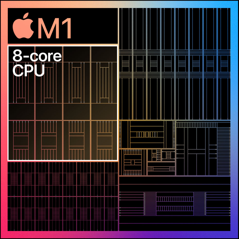
I am actually interested in the Non-Labeled part which no one on the Internet have even guessed what they are. Image Signal Processors ( ISP ), Video Decoder and Encoder, there should be a FPGA somewhere, Secure Enclave, NAND Controller, PCI-Express Controller / USB3 / Thunderbolt etc.
Mostly because all the other part are already well known.
I wonder what they'll do for "M1X" and pro-machines?
Seems like heat isn't an issue, so can they increase the clock-speed of the M1?
And will they create a larger die with 2xGPU and 2xCPUs, or will they "stitch" multiple M1 dies together on one package to have a higher yield and reduce supply chain concerns?
An M1X with 2xGPU will bring it to Radeon 5500M level which is what I have in my current 16", but still not quite to Nvidia 1080 level.
So they'll definitely need a more powerful GPU for the pro-users. I wonder if they can make a 4xGPU, or if the yield will become poor as the die size increases. Maybe they'll have to do a discrete GPU, but that doesn't seem to match their current trajectory.
And then there have been "leaks" (rumors, really) about an 32xcore M1-family CPU, but I imagine the yield of such a beast would be horrible, with all the other SOC components on the same die. Especially, if they put a 32xcore GPU on the same die.
(microelectronics graduate in 2001, turned software engineer, I have worked for ARM and Imagination Technologies on simulations of CPUs, GPUs, networking products and other bits of SoCs)
Yield wouldn't be that bad - ARM CPUs are small in comparison to their x86 cousins. I would expect that you would get to 32 CPUs the same way everyone else does - build a 32 core design and blow enable fuses on bad CPUs, then badge as appropriate.
To get a desktop class GPU they will need to address memory bandwidth. I am assuming they are using a tile based rendering process so memory bandwidth is less of an issue in comparison to scan line rendering (do desktop GPUs still do that?) I would assume that they are enjoying the benefits of the system level cache with the CPU and GPU sharing. I would expect there to be some careful benchmarking of increasing GPU cores, memory speed, memory size and system cache size going on at Apple.
There isn't anything stopping Apple from supporting external GPUs, but it would require a new SoC with more PCIe lanes. External buses are much more power hungry and take up space on the die. I don't have a mental model of how much space plonking a PCIe x16 interconnect would cost in terms of area or power (taking into account you need to get that data across the chip too), but my gut reaction is that it isn't likely unless there is a customer use case they can't solve on chip.
>Seems like heat isn't an issue, so can they increase the clock-speed of the M1?
They are running into their current node limits, so dont expect a 4Ghz+ coming unless they decide to remake the whole thing in High Performance Node. ( Which means it will cost a lot more for a relatively niche volume.)
>I wonder if they can make a 4xGPU
GPU increase should be given, and die size / yield would not be a concern / problem. The question is how will they handle the additional memory bandwidth requirement? As you can see in the Die-Shots those DDR I/O side are already take up much of the side space. Going with HBM2? Or LPDDR5?
>32xcore M1-family CPU, but I imagine the yield of such a beast would be horrible,
A 32x CPU / GPU Core M1 will only be 4x increase from its current form. If you exclude I/O part, the CPU + GPU + Cache is only a little more than 50% of die size, or ~60mm2. 4x That is only 240mm2+. The final product would be a sub 350mm2 if you include all the additional. Which is roughly inline with the current estimate of AWS Graviton 2 die size ( ~400mm2).
But yes, M1 ( A14X ) isn't really that interesting. The most exciting part is how they will go about doing high performance chip. Especially on iMac and Mac Pro.
Well, the prevailing rumor currently is a processor with 8 high-performance cores (as opposed to the 4 on the M1). I don't know if the amount of high-efficiency cores would also be doubled so that it's like 2xCPU when compared to the M1.
Yes, that's the M1X rumor, but that isn't going to be enough to compete with high-end CPUs in iMac and Mac Pros. For those, we have the 32-core rumor (but that is a massive die).
And doubling the M1-GPU will not be enough to even surpass current Macbook Pro offerings. So they'll also need to do something more on that front.
For the truly high end they will need an external GPU. Removing the integrated GPU should get up enough space for lots more Firestorm cores.
And given that Firestorm is the fastest available CPU core, they probably don’t need 32 of them to match the highest multicore performance levels of existing AMD and Intel CPUs.
I'd like to see a pro machine with daughterboard slots, allowing you to add extra CPUs. A bit like the Acorn RISC PC. I guess Apple have already done this to seom extent with the FPGA cards that you can buy for the current Mac Pro. I do wonder if that was a taste of things to come?
In short: educated guesswork. The lighter blocky regions in the die shot are recognizable as memory; a lot of the rest is based on recognizing duplicated or mirrored elements (like the two CPU1 cores) and making guesses based on their number, relative size, and what they're close to.
Identifying the GPU, for example, is based on recognizing that there are eight repeated elements within it, and matching that with the known fact that there are eight GPU cores.
You don't need an electron microscope to discern large-scale repeated structures like CPU and GPU cores, or to tell the difference between random logic and highly regular memory arrays (usually cache, but sometimes you can see microcode or register files if you look at a small enough area). An electron microscope is only useful if you want to fully reverse-engineer the entire circuit schematic, but that's overkill for basically any purpose except manufacturing your own clone.
With the right camera modifications, you don't have to remove any layers from a chip to discern the core count: https://www.flickr.com/photos/130561288@N04/48258310027/ That's an IR photograph taken with a Sony APS-C camera that the IR-blocking filter has been removed from. That's enough to make out the cores and L3 cache slices. (The rest of Fritzchens Fritz's flickr uploads are worth checking out too, especially the video showing how he preps a die for visible light photography.)
The chip design and fabrication firms have their own internal RE divisions mostly to QA their own chips. They do competitive RE, but its often less expensive for them to get a subscription to TechInsights. Economies of scale and all that.
In terms of how its done, its very proprietary. I can tell you it involves clean rooms, ion beams, electron microscopes, chemistry, and bleeding edge software.
If you want to come work for us (its enjoyable, you should :) ) check out our careers page. We are hiring like crazy in many positions.
Why not underestimate the engineering effort, could the problem is higher up in the chain (software api like Apple os) and lower (the equipment to produce the chip). Would the IP that important?
I assume you could at least make an educated guess based on the layout and ratios of the area of the caches (assuming you know their topology and sizes) and therefore their proximity to non-cache stuff.
The Cache, GPU, and NPU are all already labeled in the image.
The Secure Enclave is a good one to point out that is in the unlabeled space.
Certainly some non-DDR peripherals are in the unlabeled space, but it would be neat to have a more comprehensively labeled diagram. I wouldn't expect most peripherals to take up so many transistors compared to the processor cores.
There's probably 4 lanes of pcie to connect the nvme ssd to, a couple more lanes to run the thunderbolt controllers, 2-3 usb controllers + a hub to connect the keyboard and touchpad, an audio dac and some thermal and power usage monitoring. They might even put the ethernet controller that shoes up on the Mac mini in there.
Sorry, was looking at the marketing image. The enclave would be quite tiny though. Id say most of the undocumented part is custom glue logic which isn’t particularly identifiable.
It has a lot of roles. You have memory controllers, i/o controllers. Not sure if the SSD controllers is also part of it. Then the dedicated video encode/decode the image processing the neural engine. There's a lot of features.
Does anyone know if its possible/ tried to do ram upgrades with higher capacity chips by replacing the dram like one does in the newer chip stacked iphones?
I know nothing about chips, but I guess it's probably the last-level CPU cache but the GPU shares it as well, similar to Intel iGPU, so they decided to call it "system cache".
Sure, but what part are the L1... I can se a bunch of similar patterns to the L2/3 caches but I would like someone that knows to draw a border around them!
From a device class where the newly all-important perf per watt was always the north star, in a market with the largest chip volume, by a company with ample margins and mountains of cash? Does not seem all that absurd :)
yea it's *the world largest company (by market capitalisation), whose main product is their flagship mobile and whose main differentiator is the CPU (almost everything else is beaten or available in competing products like Camera, number of apps etc). The moment the CPU performance falls below Android devices, people will look at iPhones differently.. iOS is a differentiator but doesn't have the x factor to make iPhones justify the premium tag.
CPU speeds have been similar to competitors until around the A10 era a few years ago. The real differentiator has always been software + hardware integration happening inside the same company. The hardware team gets the insight of the software team on what areas of performance should be looked at, and the software team can optimize for the exact specifications of a future CPU line.
You’re saying The iPhone is mostly popular because the A13/14 are faster than the competition.
The grandfather points out that iPhones up to the A10 had comparable performance as the competition, and still were popular, so having faster CPUs can’t be the major reason for that popularity.
I always assumed that they would be inferior in terms of absolute performance if you were going for performance per watt. I never imagined just how efficient the silicon could be.
But these devices aren’t ‘phones’ any more are they? That’s disingenuous.
They’re hugely powerful general purpose computing devices - many people’s primary computing device if you go outside the tech bubble. They do compute intensive tasks like photo manipulation, on-line video editing, grading, and compression, they do face detection, depth estimation, etc etc.
I don’t know why people still say ‘wow all this for a telephone’ like all it does is make analog phone calls.
its a shame we can't 'dock' em to a larger monitor to do desktop work yet. There are attempts by few players, but if Apple can do that it would be another revolution..
I was pretty excited about Linux on DeX for Samsung devices since it had a capable CPU but unfortunately they discontinued it when Android 10 was released.
Right - 'one of the most powerful CPUs ever created was for a phone' sounds funny, so to get your head around it think instead 'one of the most powerful CPUs ever created was for a miniaturised 4k on-line editing suite and live broadcast system' and it doesn't sound so absurd anymore does it?
It's not absurd at all, nor surprising that the most power efficient chip was compelled by the most portable general computing device. Plugged-in desktop computers certainly weren't going to bring us here.
This just sounds like "DAE think phone=bad XD" anti-intellectualism.
I think people are misconstruing what I am saying here. I said marvel at it. It's crazy that a handheld battery powered device has one of the greatest processors in the history of human existence in it.
If you were used to using mainframes, you could have said much the same thing about desktop CPUs in the 90s. "That tiny thing doesn't even fill up a room!"
The “reports” are targeted at competitors who want to know how and what Apple did. They are quite expensive for a consumer or casual user.
The are more than just a document. A DFR includes in depth analysis, hundreds of supporting images, and usually access to the Circuit Vision for it. CV is a viewer that allows drilling into the chip down to viewing individual transistors along with the chip schematics. Think map tiles but for a chip.
> Only a die-shot, it's disappointing that there's no comment or explanation.
A die shot that Apple themselves showed at the event. Which has had the same level of annotations previously by Anantech.
Sure, the DFR in early 2021 will be much more detailed, but also expensive to the point 0.001% of HN viewers will actually be able to see it. As such, I think your skepticism of this being worthy of home page billing is not out of line.
For the record, this is not meant to be a dig at TechInsights. I’ve seen a DFR before and they really are good for what they are, it’s just not something most HNers would gain value from, even if it were free.
Kind of sad to think about this - Why does marketing dept not actually show these and instead put up a cartoonized version of Apple's chips [1]? That's in every keynote. This is a rhetorical question, the real mystery is why does an average consumer want to see unreal things to convince them its cooler/better? You'd think seeing actual die shots would be more convincing to average consumer, but they love marketing that's untruthful, fake and exaggerated. Not the fault of the marketing department. This is what consumers want and this is what sells. Sad to think how shiny things sell and the whole luxury industry in general.
They do have a shot on https://www.apple.com/mac/m1/ (the first non-logo image) which looks like it matches up (you'll need to rotate one by 180°). So it's not like they're hiding it or actively avoiding it. It apparently just doesn't suit their needs.
The degree to which they hype UMA (a term of art within the PC industry for decades) on that page is amusing --- if Intel did the same sort of marketing for its integrated GPUs, they would almost certainly be laughed at.
From what I've read it seems to be different from Intel's UMA. It's cache-friendly single pool of memory directly accessible from different cores of the SoC: CPU, GPU, NPU etc. Since there's no division of RAM between different parts of the SoC, copying operations aren't needed.
I also read somewhere that they made sure the data formats used by the various modules are identical. Without that, you have to copy data to do format conversions. I don’t know how much of a problem that is in general, though.
M1's performance is great, but there isn't much evidence to attribute it to the memory subsystem. Also, people wanting to fit 32GB worth of apps into 16GB is just wishful thinking that isn't supported by evidence either.
Quite a lot of testing in Final Cut and Logic etc showing very good performance and efficient swap. So for most consumer apps it works well. No magic if you need a big block of memory for ML or analytics.
Do we know what benefit they're getting by putting the memory on the chip to begin with? I had initially assumed there was some non-trivial performance advantage in it, but now people are saying not so much, so why did they do it?
It seems weird to artificially limit the max memory if there was no advantage in it.
As a technical consumer I don’t know why I would want to see the actual die shots - it really doesn’t tell me anything at all.
The graphics they put on slides or marketing sites aren’t supposed to be technical reference material, usually it’s just about conveying the idea of a SoC or performance improvements, or relative sizes, or whatever.
For some people yes, for others it’s a confusing jumble of fuzzy shapes that distract them from the pertinent information. I think Apple approach of providing simplified diagrams, and also illustrative die shots (yes, they did provide die shots, so the whole premise of this discussion is stupid) was perfectly fine.
Isn't a big idea of diagrams that they aren't real so can be simpler and easier to understand? Otherwise we'd just use photos or actual schematics.
> more inspiring
Most people just need to get the info so they can get on with their job and day and get home to their kids. They aren't looking to be inspired right now. That's fine.
The inquiry I am making is more general - infantilization of consumers and the idea of dumbing things down for consumers like they're blobs of meat with cash to spare.
You don't need to see the cartoonized version of it either. May be its easier as a schematic to explain? Not sure. A list of M1's features would work equally well. I think its just marketing pizzaz.
Your refusal to take a moment to think why Apple’s marketing team did this is very funny. Do you think they just throw a dart into a spinning board when making decisions like this? There’s a difference between “dumbing” things down and effectively conveying your messages. Suggesting that they include an actual die shot in their ads for general consumers is one of the most HN-esque comments I read this month.
Though there’s still the possibility that they could add it into the detailed specifications page, or perhaps even a link in the footnotes of the specifications page? Surely that would be a better match for the target audience that would care.
Apple isn't an education company so it shouldn't be surprising their marketing department doesn't worry about simplifying things for their real goals. At the end of the day the customers are blobs of meat with cash to spare and the advertisement is to change the latter part not teach the former.
Does it make a difference? The ones from the marketing department convey the message better and are pretty to look at. These are not as cool to average consumer.
The other discussion here recently about how Apple is very silo'd internally is relevant: the marketing department very likely doesn't have access to real die photos.
They're in a weird spot. They're obviously making a lot of money, but most companies in their position do a lot of work to court developers and accessory makers etc. Apple's position is essentially that they control the market so you need them more than they need you.
But that makes others resent them. Which is a vulnerability because it means you have all the rest of the industry ready to sell Apple down the river the first chance they get, whether it's in making antitrust claims or lobbying against them or just fervently supporting any half viable competitor in the hopes that it becomes fully viable.
This is how it seems to me too. I still have their hardware I got years ago and it works great, but it's been a couple of years since I've decided to refuse any software upgrades from them, and to avoid their hardware. Their attitude seems to be getting more and more "our way or the highway", and I'm not interested in playing those games.
Previously I already switched from Windows to Mac as my primary environment, so going to GNU/*ix was not a big stretch. I already know several non-hackers who have gone this route as well.
Depending on what the community is looking to know, there may be some things we can share publicly. I’m in the software group and not intimately involved with the RE parts, but I will act as an ambassador and see if I can get the right people involved.
Throw some comments on this thread and we’ll see what we can do to help. Might be next week due to holidays.