There's some pretty famous "signs" that companies would put into their chips to show that it was blatently stolen. Also at some point it became a game:
What's fascinating is that you can basically run a country with little to no "actual" development of computer hardware, and just have an entire industry around "copying" to keep yourself up to date (or a few years behind at most).
This is pretty evident with China of the past few years in military tech, and now they are starting to leap frog (See engine issues with their new fighter, and how they are almost there but not quite. Russia is unwilling to sell them newer engines for fear of copying essentially)
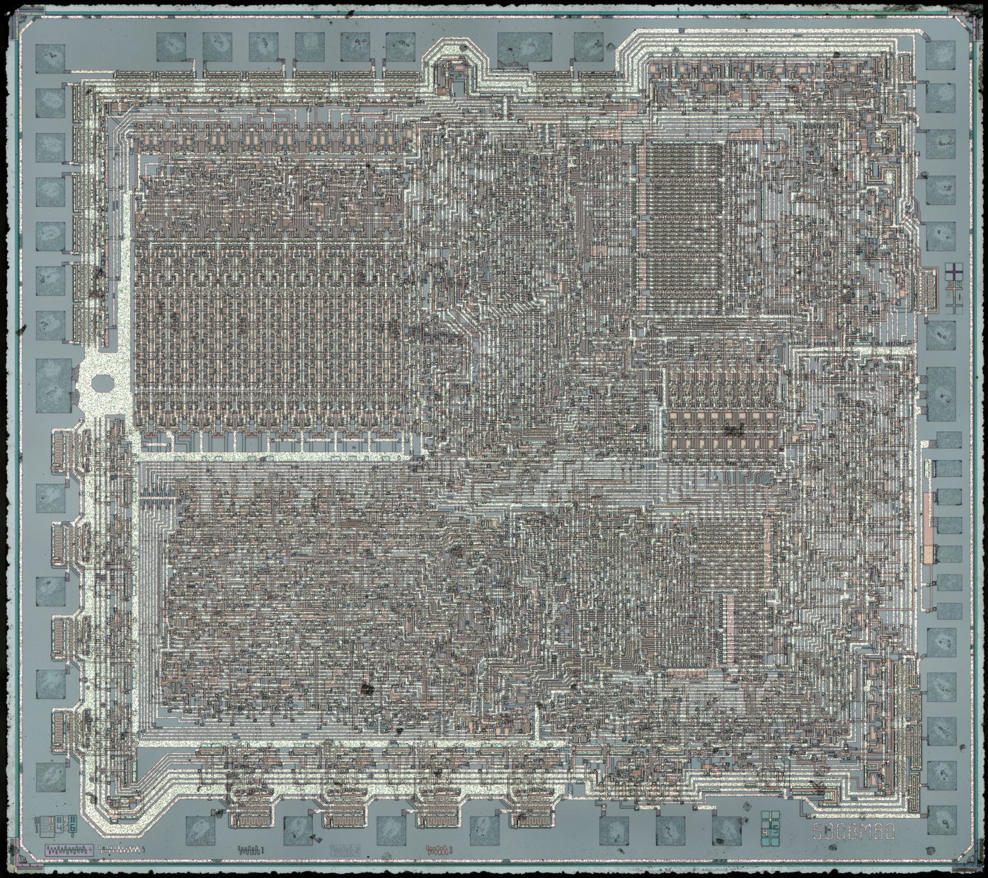
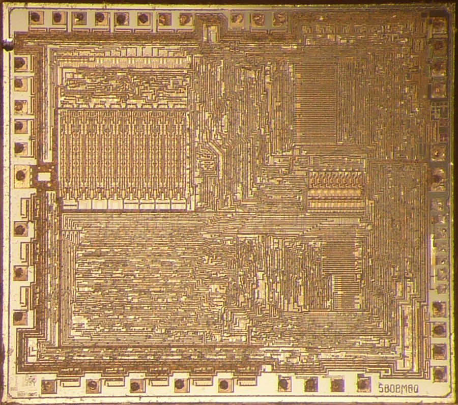
I am not an expert in CPU design, so please correct me if i am wrong, but chips look rather different (at least Intel logo was removed on the 580BM80A die). Could it be that 580BM80A implements Intel's ISA, but actual CPU architecture is of their own? And could we call it a "copy"/"replica" if so? Like could we say that AMD CPUs are replicas of Intel CPUs, because they implement the same ISA?
Those two chips are a lot more different than I'd expect. (Even taking into account the 90 degree rotation.) In particular, the ALU (upper-left in Intel photo) is fairly regular, while the ALU in the Russian photo (lower-left) looks like random logic. And the PLAs and instruction register seem entirely different between the two.
I was skeptical at first, but I think it's possible that the Russian chip is a different implementation, and not just the same circuitry with the layout re-done for their process. It would require a closer look at the circuitry to determine for sure.
Most likely the same way how enthusiasts are reverse-engineering those 8-bit CPUs today: decapping and tracing the transistors under a microscope.
For the East German Z80 clone U880 there are some wild stories of how the secret service stole blueprints from Zilog, but the more believable version of the story is that some chips were smuggled over the border that had simply been bought in West German electronics stores. The East German Z80 version had definitely been reverse engineered - not simply cloned - because the U880 has a slightly different undocumented behaviour (for instance, the undocumented X and Y flags behave differently than on a real Z80), also apparently the Z80 has various 'trap transistors' which prevent that the mask can simply be cloned, those trap transistors had to be found and fixed (I guess this was the reason why the U880 project was delayed by a year or so).
The much bigger problem than reverse engineering the chips was setting up manufacturing anyway. For East Germany this definitely happened with secret service support. The story goes that a small chip manufacturing company was set up in West Germany, which soon after declared bancrupty with the entire manufacturing equipment sold off to another company somewhere abroad. "Somehow" that equipment disappeared en route and showed up in East Germany a few months later.
And the absolutely amazing gem. In 1983 legendary science education TV program SONDA documented design and manufacturing of first batches in a humorous lets bake a cake fashion. Paper plotters, light pens, developing/rinsing dies by hand, electron miscroscope debugging, the whole nine yards!
It's my understanding that photos of a semiconductor die (pre-CMOS) aren't 100% useful, since often the sizes of transistors relative to one another becomes an important detail, which is hard to extrapolate to standard logic gates. It's my understanding that the Motorola 68000 still has some outstanding emulation problems (related to the instruction cache), due to using HMOS logic. NMOS chips like the 8080 are also affected by this.
Transistor sizes are easy to extract from photos. What's hard is doping levels, which can make a transistor enhancement or depletion. The type is usually obvious from context. However, the Z-80 designers famously used the "wrong" doping for a few transistors. The purpose of this was to create traps for companies copying the IC from the die, since a straightforward copy would yield a few gates that didn't work right.
I've found a few of these traps in the Z-80, and they were placed very maliciously. The circuit appears reasonable and correct, but fails in subtle ways.
> It's my understanding that the Motorola 68000 still has some outstanding emulation problems (related to the instruction cache), due to using HMOS logic.
This doesn't sound right to me. For one thing, the idea that you need to simulate analog effects in order to properly emulate an instruction cache sort of flies in the face of my (admittedly amateur) understanding of reasonable chip design. For another, that'd imply that the CMOS versions of the 68K function differently than the HMOS ones, and I can't find any indication of that. Finally, as far as I know the 68000 doesn't have an instruction cache!
There were no any problems to recognize n-MOS logic during the reverse - everything was quite obvious regardless the transistor sizes. And I just dropped the sizes in my schematics, it simplified the process a lot.
As a person not fluent in processor design, chip design, FPGAs or Verilog, is there some demonstration of actual software running on this implementation? Or is that one or more steps away after synthesising and loading the bitstream in to the FPGA?
In the tst directory they have .asm files, which they load in the program memory to test the CPU. The abstract mentions that they run it in FPGA, but it wouldn't be difficult to run those tests in simulation too (albeit exceedingly slow).
Setun used balanced ternary logic instead of binary logic. Each trit could be -1, 0, or +1. For numeric values, there was no need to store a sign, since the sign of a number would be inherent in its ternary value.
Then the Soviets decided that it would be easier and faster to just copy western computers, and the concept wasn't developed any further.
USSR made an incompatible "clone" of Apple-II, called AGAT with better graphics. Also 8086 clone VM86 AFAIK was significantly reingennered. Some PDP-11 clones were also designed from the scratch.
It could mean either. Rad-hard parts are used in satellites. I am not familiar with the current crop of rad-hard parts.
I did work as a CPU logic desiger at Amdahl. We had full parity through-checking, so an ALU intermittent logic error would raise a parity exception. Certainly IBM would have had the same, it was standard SOTA reliability logic for the era of mainframes when I was a designer.